DS90C032W-QML National Semiconductor, DS90C032W-QML Datasheet
DS90C032W-QML
Specifications of DS90C032W-QML


Related parts for DS90C032W-QML

DS90C032W-QML Summary of contents
Page 1
... LVDS inputs. This feature assures minimal load- ing effect on the LVDS bus lines when V Ordering Information NS Part Number SMD Part Number DS90C032E-QML DS90C032W-QML DS90C032WG-QML DS90C032W-QMLV DS90C032WG-QMLV DS90C032WLQMLV DS90C032WGLQMLV TRI-STATE ® registered trademark of National Semiconductor Corporation. © 2007 National Semiconductor Corporation Features ■ ...
Page 2
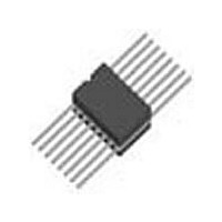
Connection Diagrams Dual-In-Line Pictured See NS Package Number W16A & WG16A Functional Diagram and Truth Tables Receiver EN L All other combinations of ENABLE inputs www.national.com 20163701 20163702 ENABLES INPUTS EN* R − ≥ V 0.1V ...
Page 3
... JC LCC Package Ceramic Flatpack Ceramic SOIC ESD Rating (Note 3) Recommended Operating Conditions Supply Voltage ( Receiver Input Voltage Operating Free Air Temperature ( Radiation Features DS90C032WLQMLV DS90C032WGLQMLV (Note 1) Min +4.5V Gnd −55°C 3 −0.3V to +6V −0. +0.3V) CC −0. +0.3V) CC −0. +0.3V) CC ≤ ...
Page 4
Quality Conformance Inspection Mil-Std-883, Method 5005 - Group A Subgroup Parameters (Note 7) Symbol Parameter V Differential Input Low Threshold V ThL V Differential ...
Page 5
AC Parameters (Note 7) The following conditions apply, unless otherwise specified. AC 4.5V / 5.0V / 5.5V Symbol Parameter t Differential Propagation Delay PHLD High to Low t Differential Propagation Delay PLHD Low to High ...
Page 6
Parameter Measurement Information FIGURE 1. Receiver Propagation Delay and Transition Time Test Circuit FIGURE 2. Receiver Propagation Delay and Transition Time Waveforms C includes load and test jig capacitance for t and t measurements ...
Page 7
FIGURE 4. Receiver TRI-STATE Delay Waveforms Typical Performance Characteristics Output High Voltage vs Power Supply Voltage Output Low Voltage vs Power Supply Voltage Output High Voltage vs Ambient Temperature 20163708 Output Low Voltage vs Ambient Temperature 20163710 7 20163706 20163709 ...
Page 8
Output Short Circuit Current vs Power Supply Voltage Differential Propagation Delay vs Power Supply Voltage Differential Skew vs Power Supply Voltage www.national.com Output Short Circuit Current vs Ambient Temperature 20163712 Differential Propagation Delay vs Ambient Temperature 20163714 Differential Skew vs ...
Page 9
Transition Time vs Power Supply Voltage Typical Application Applications Information LVDS drivers and receivers are intended to be primarily used in an uncomplicated point-to-point configuration as is shown in Figure 5. This configuration provides a clean signaling en- vironment for ...
Page 10
Revision History Released Revision 03/01/06 A New Release, Corporate format 10/10/06 B Applications Information - Pg. 10, Physical Dimensions - Pg. 12 05/07/07 C Receiver Table - Pg. 2, Application Information - Pg. 9 & 10 www.national.com Section Originator L. ...
Page 11
Physical Dimensions inches (millimeters) unless otherwise noted 20-Lead Ceramic Leadless Chip Carrier NS Package Number E20A 16-Lead Ceramic Flatpack NS Package Number W16A 11 www.national.com ...
Page 12
Ceramic SOIC NS Package Number WG16A 12 ...
Page 13
Notes 13 www.national.com ...
Page 14
... National Semiconductor and the National Semiconductor logo are registered trademarks of National Semiconductor Corporation. All other brand or product names may be trademarks or registered trademarks of their respective holders. ...