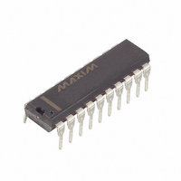
DS2186 Maxim Integrated Products, DS2186 Datasheet - Page 3

DS2186
Manufacturer Part Number
DS2186
Description
IC TRANSMIT LINE INTERFACE 20DIP
Manufacturer
Maxim Integrated Products
Type
Line Driver, Transmitterr
Datasheet
1.DS2186S.pdf
(11 pages)
Specifications of DS2186
Number Of Drivers/receivers
1/0
Protocol
T1/CEPT
Voltage - Supply
4.75 V ~ 5.25 V
Mounting Type
Through Hole
Package / Case
20-DIP (0.300", 7.62mm)
Lead Free Status / RoHS Status
Contains lead / RoHS non-compliant
Available stocks
Company
Part Number
Manufacturer
Quantity
Price
Part Number:
DS2186
Manufacturer:
DALLAS
Quantity:
20 000
Part Number:
DS2186S
Manufacturer:
DALLAS
Quantity:
20 000
Company:
Part Number:
DS2186S+
Manufacturer:
Maxim Integrated Products
Quantity:
135
PIN DESCRIPTION Table 1
INPUT DATA MODES
Input data is sampled on the falling edge of TCLK or
LCLK and can be bipolar (dual rail) or unipolar (single
rail, NRZ). TPOS, TNEG and TCLK are the data and
clock inputs when LB=0, LPOS, LNEG and LCLK when
LB=1. TPOS and TNEG (LPOS and LNEG) must be tied
together in NRZ applications.
ZERO CODE SUPPRESSION MODES
Transmitted data is treated transparently (no zero code
suppression) when ZCSEN=0. HDB3 code words re-
place any all–zero nibble when ZCSEN=1 and
TCLKSEL=1. B8ZS code words replace any incoming
all–zero byte when ZCSEN=1 and TCLKSEL=0.
PIN
10
12
13
14
15
16
17
18
19
20
11
1
2
3
4
5
6
7
8
9
TCLKSEL
SYMBOL
MRING,
ZCSEN
TRING
TNEG,
LNEG,
TPOS
LPOS
LEN0
LEN1
LEN2
TCLK
LCLK
TTIP,
MTIP
TAIS
V
V
LF
LB
DD
SS
TYPE
O
O
–
–
I
I
I
I
I
I
I
I
I
I
Transmit Alarm Indication Signal. When high, output data is
forced to all ones at the TCLK (LB=0) or LCLK (LB=1) rate.
Zero Code Suppression Enable. When high, B8ZS or HDB3
encoder enabled.
Transmit Clock Select. Tie to V
tions, to V
Length Select 0, 1 and 2. State determines output T1 waveform
shape and characteristics.
Positive Supply. 5.0 volts.
Transmit Tip and Ring. Line driver outputs; connect to transmit
line transformer.
Signal Ground. 0.0 volts.
Line Fault. Open collector active low output. Held low during an
output driver fault and/or failure; tri–stated otherwise.
Monitor Tip and Ring. Normally connected to TTIP and TRING.
Sense inputs for line fault detection circuitry.
Loopback. When high, input data is sampled at LPOS and LNEG
on falling edges of LCLK; when low, input data is sampled at TPOS
and TNEG on falling TCLK.
Transmit Data. Sampled on falling edges of TCLK when LB=0.
Transmit Clock. 1.544 MHz or 2.048 MHz primary data clock.
Loopback Data. Sampled on falling edges of LCLK when LB=1.
Loopback Clock. 1.544 MHz or 2.048 MHz loopback data clock.
DD
for 2.048 MHz (CEPT) applications.
ALARM INDICATION SIGNAL
When TAIS is set, an all ones code is continuously
transmitted at the TCLK rate (LB=0) or the LCLK rate
(LB=1).
WAVE SHAPING
The device supports T1 short loop (DSX–1; 0 to 655
feet), T1 long loop (CSU; 0 dB, –7.5 dB and –15 dB) and
CEPT (CCITT G.703) pulse template requirements.
On–chip laser trimmed delay lines clocked by either
TCLK or LCLK control a precision digital–to–analog
converter to build the desired waveforms, which are
buffered differentially by the line drivers.
DESCRIPTION
SS
for 1.544 MHz (T1) applica-
022798 3/11
DS2186


