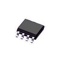
MAX9633ASA+ Maxim Integrated Products, MAX9633ASA+ Datasheet - Page 2

MAX9633ASA+
Manufacturer Part Number
MAX9633ASA+
Description
Op Amps Dual High-Voltage Op Amp
Manufacturer
Maxim Integrated Products
Datasheet
1.MAX9633ATA.pdf
(14 pages)
Specifications of MAX9633ASA+
Number Of Channels
2
Voltage Gain Db
140 dB
Common Mode Rejection Ratio (min)
105 dB
Input Voltage Range (max)
13.3 V
Input Voltage Range (min)
- 15 V
Input Offset Voltage
70 uV
Operating Supply Voltage
4.5 V to 36 V
Supply Current
3.5 mA
Maximum Power Dissipation
1951.2 mW
Maximum Operating Temperature
+ 125 C
Mounting Style
SMD/SMT
Package / Case
SOIC-8
Maximum Dual Supply Voltage
18 V
Minimum Operating Temperature
- 40 C
Lead Free Status / Rohs Status
Details
SO-EP
Dual 36V Op Amp for 18-Bit
SAR ADC Front-End
ABSOLUTE MAXIMUM RATINGS
Supply Voltage (V
All Other Pins ..................................(V
Short-Circuit Duration of OUTA, OUTB ................................. 10s
Continuous Input Current (any pins) ............................... ±20mA
Continuous Power Dissipation (T
Note 1: Package thermal resistances were obtained using the method described in JEDEC specification JESD51-7, using a four-
ELECTRICAL CHARACTERISTICS
(V
T
PACKAGE THERMAL CHARACTERISTICS (Note 1)
Stresses beyond those listed under “Absolute Maximum Ratings” may cause permanent damage to the device. These are stress ratings only, and functional
operation of the device at these or any other conditions beyond those indicated in the operational sections of the specifications is not implied. Exposure to absolute
maximum rating conditions for extended periods may affect device reliability.
2
POWER SUPPLY
Supply Voltage Rang
Supply Current
Power-Supply Rejection Ratio
DC SPECIFICATIONS
Input Offset Voltage
Input Offset Voltage Drift
(Note 3)
Input Bias Current
Input Offset Current
Input Voltage Range
Common-Mode Rejection Ratio
A
Junction-to-Ambient Thermal Resistance (q
Junction-to-Case Thermal Resistance (q
CC
SO (derate 24.4mW/NC above +70NC)
Multilayer Board .....................................................1951.2mW
= +25NC.) (Note 2)
= +15V, V
layer board. For detailed information on package thermal considerations, refer to www.maxim-ic.com/thermal-tutorial.
PARAMETER
EE
CC
= -15V, V
to V
e
EE
).................................-0.3V to +40V
CM
A
= 0V, R
= +70NC)
V
V
EE
SYMBOL
CC
IN+
CMRR
PSRR
DV
V
- 0.3V) to (V
I
I
L
CC
OS
I
OS
B
, V
- V
OS
= 10kI to V
JC
IN-
EE
) .................7°C/W
JA
) ..........41°C/W
Guaranteed by PSRR
Per amplifier
+4.5V P (V
P +36V
T
-40NC P T
-40NC P T
(V
V
(V
V
Guaranteed by CMRR
V
V
+125NC
A
EE
EE
EE
EE
EE
EE
CC
= +25NC
P V
P V
P V
P V
GND
+ 0.45V) P V
+ 0.45V) P V
+ 0.3V)
CM
CM
CM
CM
A
CC
A
= 0V, T
P +125NC
P (V
P (V
P (V
P (V
P +125NC
- V
CONDITIONS
EE
CC
CC
CC
CC
)
CM
CM
A
- 1.8V)
- 1.8V)
- 1.7V), T
- 1.8V), -40NC P T
Operating Temperature Range ........................ -40NC to +125NC
Junction Temperature .....................................................+150NC
Storage Temperature Range ............................ -65NC to +150NC
Soldering Temperature (reflow) ......................................+260NC
TDFN-EP
= T
P (V
P (V
T
-40NC P T
-40NC P T
T
-40NC P T
TDFN (derate 24.4mW/NC above +70NC)
Multilayer Board ........................................................1905mW
Junction-to-Ambient Thermal Resistance (q
Junction-to-Case Thermal Resistance (q
A
A
MIN
= +25NC
= +25NC
CC
CC
T
-40NC P T
+125NC
A
to T
A
- 1.8V)
- 1.8V)
= +25NC
= +25NC
A
A
A
MAX
P +85NC
P +125NC
P +125NC
A
, unless otherwise noted. Typical values are at
A
P
P
MIN
V
V
112
110
106
105
4.5
EE
EE
Q200
TYP
135
Q70
Q42
Q30
130
130
3.5
0.2
4.5
JC
) .................8°C/W
Q2000
JA
V
V
Q200
Q290
Q400
Q300
MAX
6.5
0.9
1.7
1.8
CC
CC
36
22
5
6
) ..........42°C/W
-
-
UNITS
FV/NC
mA
dB
nA
FA
nA
dB
FV
V
V


