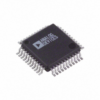
ADV7177KS-REEL Analog Devices Inc, ADV7177KS-REEL Datasheet - Page 13

ADV7177KS-REEL
Manufacturer Part Number
ADV7177KS-REEL
Description
IC DAC VIDEO NTSC 3-CH 44MQFP
Manufacturer
Analog Devices Inc
Type
Video Encoderr
Datasheet
1.ADV7177KSZ-REEL.pdf
(44 pages)
Specifications of ADV7177KS-REEL
Rohs Status
RoHS non-compliant
Applications
Set-Top Boxes, TV
Voltage - Supply, Analog
3 V ~ 3.6 V
Mounting Type
Surface Mount
Package / Case
44-MQFP, 44-PQFP
Adc/dac Resolution
9b
Screening Level
Commercial
Package Type
MQFP
Pin Count
44
Voltage - Supply, Digital
-
Lead Free Status / RoHS Status
Not Compliant
PIN CONFIGURATION AND FUNCTION DESCRIPTIONS
Table 9. Pin Function Descriptions
Pin No.
1, 20, 28, 30
2
3 to 10,
12 to 14,
37 to 41
11
15
16
17
18
19, 21, 29, 42
22
23
24
25
26
27
31
32
33
34–36
43
44
Mnemonic
V
CLOCK/2
P5 to P12,
P13 to 14,
P0 to P4
OSD_EN
HSYNC
FIELD/
VSYNC
BLANK
ALSB
GND
RESET
SCLOCK
SDATA
COMP
DAC C
DAC B
DAC A
V
R
OSD_0 to
OSD_2
CLOCK
CLOCK
AA
REF
SET
I/O
P
O
I
I
I/O
I/O
I/O
I
G
I
I
I/O
O
O
O
O
I/O
I
I
O
I
Function
Power Supply.
Synchronous Clock Output Signal. Can be either 27 MHz or 13.5 MHz; this can be controlled by MR32
and MR33 in Mode Register 3.
8-Bit, 4:2:2 Multiplexed YCrCb Pixel Port (P7–P0) or 16-Bit YCrCb Pixel Port (P15–P0). P0 represents the
LSB.
Enables OSD input data on the video outputs.
HSYNC (Modes 1 and 2) Control Signal. This pin can be configured to output (master mode) or accept
(slave mode) Sync signals.
Dual Function Field (Mode 1) and VSYNC (Mode 2) Control Signal. This pin can be configured to
output (master mode) or accept (slave mode) these control signals.
Video Blanking Control Signal. The pixel inputs are ignored when this is Logic 0. This signal is optional.
TTL Address Input. This signal sets up the LSB of the MPU address.
Ground Pin.
The input resets the on-chip timing generator and sets the ADV7177/ADV7178 into default mode. This
is NTSC operation, Timing Slave Mode 0, 8-bit operation, 2× composite and S VHS out.
MPU Port Serial Interface Clock Input.
MPU Port Serial Data Input/Output.
Compensation Pin. Connect a 0.1 µF capacitor from COMP to V
DAC C Analog Output.
DAC B Analog Output.
DAC A Analog Output.
Voltage Reference Input for DACs or Voltage Reference Output (1.235 V).
A 300 Ω resistor connected from this pin to GND is used to control full-scale amplitudes of the video
signals.
On Screen Display Inputs.
Crystal Oscillator Output (to crystal). Leave unconnected if no crystal is used.
Crystal Oscillator Input. If no crystal is used, this pin can be driven by an external TTL clock source; it
requires a stable 27 MHz reference clock for standard operation. Alternatively, a 24.5454 MHz (NTSC)
or 29.5 MHz (PAL) can be used for square pixel operation.
CLOCK/2
OSD_EN
V
P10
P12
P11
AA
P5
P6
P7
P8
P9
10
11
1
2
3
4
5
6
7
8
9
44 43 42 41 40 39 38 37 36 35 34
12 13 14 15 16 17 18 19 20 21 22
PIN 1
Figure 6. Pin Configuration
AD7177/ADV7178
Rev. C | Page 13 of 44
(Not to Scale)
TOP VIEW
MQFP
33
32
31
30
29
28
27
26
25
24
23
R
V
DAC A
V
GND
V
DAC B
DAC C
COMP
SDATA
SCLOCK
REF
AA
AA
SET
AA
.
ADV7177/ADV7178


