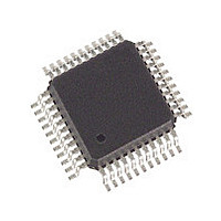
SAF7129AH/V1,518 NXP Semiconductors, SAF7129AH/V1,518 Datasheet - Page 30

SAF7129AH/V1,518
Manufacturer Part Number
SAF7129AH/V1,518
Description
IC DIGITAL VIDEO ENCODER 44-QFP
Manufacturer
NXP Semiconductors
Type
Video Encoderr
Datasheet
1.SAF7129AHV1518.pdf
(56 pages)
Specifications of SAF7129AH/V1,518
Package / Case
44-QFP
Voltage - Supply, Analog
3.15 V ~ 3.45 V
Voltage - Supply, Digital
3 V ~ 3.6 V
Mounting Type
Surface Mount
Maximum Operating Temperature
+ 85 C
Minimum Operating Temperature
- 40 C
Mounting Style
SMD/SMT
Lead Free Status / RoHS Status
Lead free / RoHS Compliant
Applications
-
Lead Free Status / Rohs Status
Compliant
Other names
935274073518
SAF7129AH/V1-T
SAF7129AH/V1-T
SAF7129AH/V1-T
SAF7129AH/V1-T
Available stocks
Company
Part Number
Manufacturer
Quantity
Price
Company:
Part Number:
SAF7129AH/V1,518
Manufacturer:
Sigma Designs Inc
Quantity:
10 000
Philips Semiconductors
Table 50 Subaddress 6BH
Table 51 Selection of the signal type on pin RCV1
2004 Mar 16
Digital video encoder
SRCV11
BIT
7
6
5
4
3
2
1
0
0
0
1
1
SYMBOL
SRCV11
SRCV10
SRCV10
ORCV1
ORCV2
PRCV1
PRCV2
TRCV2
CBLF
0
1
0
1
These 2 bits define signal type on pin RCV1; see Table 51
0 = horizontal synchronization is taken from RCV1 port (at bit SYMP = LOW) or from
decoded frame sync of “ITU-R BT.656” input (at bit SYMP = HIGH); default state after
reset
1 = horizontal synchronization is taken from RCV2 port (at bit SYMP = LOW)
0 = pin RCV1 is switched to input; default state after reset
1 = pin RCV1 is switched to output
0 = polarity of RCV1 as output is active HIGH, rising edge is taken when input; default
state after reset
1 = polarity of RCV1 as output is active LOW, falling edge is taken when input
When CBLF = 0.
When CBLF = 1.
0 = pin RCV2 is switched to input; default state after reset
1 = pin RCV2 is switched to output
0 = polarity of RCV2 as output is active HIGH, rising edge is taken when input,
respectively; default state after reset
1 = polarity of RCV2 as output is active LOW, falling edge is taken when input,
respectively
If ORCV2 = 1, pin RCV2 provides an HREF signal (horizontal reference pulse that is
defined by RCV2S and RCV2E, also during vertical blanking interval); default state
after reset.
If ORCV2 = 0 and bit SYMP = 0, signal input to RCV2 is used for horizontal
synchronization only (if TRCV2 = 1); default state after reset.
If ORCV2 = 1, pin RCV2 provides a ‘composite-blanking-not’ signal, for example a
reference pulse that is defined by RCV2S and RCV2E, excluding vertical blanking
interval, which is defined by FAL and LAL.
If ORCV2 = 0 and bit SYMP = 0, signal input to RCV2 is used for horizontal
synchronization (if TRCV2 = 1) and as an internal blanking signal.
RCV1
FSEQ
VS
FS
Vertical Sync each field; default state after reset
Frame Sync (odd/even)
Field Sequence, vertical sync every fourth field (PAL = 0), eighth field
(PAL = 1) or twelfth field (SECAM = 1)
not applicable
30
DESCRIPTION
FUNCTION
SAF7129AH
Product specification


