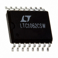
LTC1062CSW#PBF Linear Technology, LTC1062CSW#PBF Datasheet - Page 6

LTC1062CSW#PBF
Manufacturer Part Number
LTC1062CSW#PBF
Description
IC FILTR 5TH ORDR LOWPASS 16SOIC
Manufacturer
Linear Technology
Datasheet
1.LTC1062CN8PBF.pdf
(16 pages)
Specifications of LTC1062CSW#PBF
Filter Type
Butterworth, Lowpass Switched Capacitor
Frequency - Cutoff Or Center
20kHz
Number Of Filters
1
Max-order
5th
Voltage - Supply
5 V ~ 16 V, ±2.5 V ~ 8 V
Mounting Type
Surface Mount
Package / Case
16-SOIC (0.300", 7.5mm Width)
Ic Filter Type
Switched Capacitor
Filter Order
5th
No. Of Filters
1
Cutoff Frequency
20kHz
Program Clock Frequency Typ
4MHz
Supply Voltage Range
± 2.5V To ± 9V
Rohs Compliant
Yes
Lead Free Status / RoHS Status
Lead free / RoHS Compliant
Available stocks
Company
Part Number
Manufacturer
Quantity
Price
APPLICATIO S I FOR ATIO
Filter Input Voltage Range
Every node of the LTC1062 typically swings within 1V of
either voltage supply, positive or negative. With the appro-
priate external (RC) values, the amplitude response of all
the internal or external nodes does not exceed a gain of
0dB with the exception of Pin 1. The amplitude response
of the feedback node (Pin 1) is shown in Figure 2. For an
input frequency around 0.8 • f
±5V supplies, the peak-to-peak input voltage should not
exceed 4.7V. If the input voltage goes beyond this value,
clipping and distortion of the output waveform occur, but
the filter will not get damaged nor will it oscillate. Also, the
absolute maximum input voltage should not exceed the
power supplies.
Internal Buffer
The internal buffer out (Pin 8) and Pin 1 are part of the
signal AC path. Excessive capacitive loading will cause
gain errors in the passband, especially around the cutoff
frequency. The internal buffer gain at DC is typically
0.006dB. The internal buffer output can be used as a filter
output, however, it has a few millivolts of DC offset. The
temperature coefficient of the internal buffer is typically
1µV/°C.
Filter Attenuation
The LTC1062 rolloff is typically 30dB/octave. When the
clock and the cutoff frequencies increase, the filter’s
maximum attenuation decreases. This is shown in the
6
LTC1062
–10
–12
–14
–2
–4
–6
–8
Figure 2. Amplitude Response of Pin 1
6
4
2
0
0.1
U
U
f
IN
1
/f
C
C
, the gain is 1.7V/V and, with
V
2πRC
W
S
1
= ±5V
=
1062 F02
1.62
f
C
10
U
Typical Performance Characteristics. The decrease of the
maximum attenuation is due to the rolloff at higher
frequencies of the loop gains of the various internal
feedback paths and not to the increase of the noise floor.
For instance, for a 100kHz clock and 1kHz cutoff fre-
quency, the maximum attenuation is about 64dB. A 4kHz,
1V
at the output. A 6kHz, 1V
ated by 64dB and not by 77dB as an ideal 5th order
maximum flat filter would have dictated. The LTC1062
output at 6kHz will be about 630µV
RMS noise from DC to 17kHz was 100µV
16dB below the filter output.
C
The C
C
it should be connected from Pin 5 to the negative supply,
Pin 3. C
Pin 5 is floating, an internal 33pF capacitor plus the
external interpin capacitance set the oscillator frequency
around 140kHz with ±5V supply. An external C
bring the oscillator frequency down by the ratio (33pF)/
(33pF + C
curves provide the necessary information to get the inter-
nal oscillator frequency for various power supply ranges.
Pin 5 can also be driven with an external CMOS clock to
override the internal oscillator. Although standard 7400
series CMOS gates do not guarantee CMOS levels with the
current source and sink requirements of Pin 5, they will, in
reality, drive the C
standard B series output drive have the appropriate volt-
age levels and more than enough output current to
simultaneously drive several LTC1062 C
typical trip levels of the internal Schmitt trigger which
input is Pin 5, are given in Table 1.
Table 1
OSC
OSC
RMS
, Pin 5
, connected from Pin 5 to ground. If C
OSC
V
±2.5V
SUPPLY
input signal will be predictably attenuated by 60dB
±5V
±6V
±7V
OSC
, Pin 5, can be used with an external capacitor,
OSC
lowers the internal oscillator frequency. If
). The Typical Performance Characteristics
OSC
pin. CMOS gates conforming to
RMS
1.75V
V
0.9V
1.3V
1.7V
TH
+
input signal will be attenu-
RMS
. The measured
OSC
OSC
RMS
–2.1V
–2.5V
–2.9V
is polarized
V
–1V
TH
pins. The
which is
–
OSC
1062fd
will


