NTMFS4933NT1G ON Semiconductor, NTMFS4933NT1G Datasheet
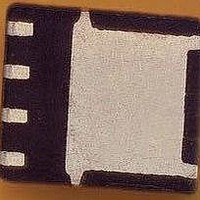
MOSFET N-CH 30V 232A SO8 FL

NTMFS4933NT1G

Manufacturer Part Number
NTMFS4933NT1G
Description
MOSFET N-CH 30V 232A SO8 FL
Manufacturer
ON Semiconductor
Series
-r
Datasheet

Specifications of NTMFS4933NT1G

Fet Type
MOSFET N-Channel, Metal Oxide
Fet Feature
Logic Level Gate
Rds On (max) @ Id, Vgs
1.2 mOhm @ 30A, 10V
Drain To Source Voltage (vdss)
30V
Current - Continuous Drain (id) @ 25° C
20A
Vgs(th) (max) @ Id
2.2V @ 250µA
Gate Charge (qg) @ Vgs
62.1nC @ 4.5V
Input Capacitance (ciss) @ Vds
10930pF @ 15V
Power - Max
950mW
Mounting Type
*
Package / Case
*
Configuration
Single
Transistor Polarity
N-Channel
Resistance Drain-source Rds (on)
2 mOhms
Forward Transconductance Gfs (max / Min)
82 S
Drain-source Breakdown Voltage
30 V
Continuous Drain Current
34 A
Power Dissipation
2.74 W
Mounting Style
SMD/SMT
Fall Time
23 ns
Gate Charge Qg
62.1 nC
Rise Time
33 ns
Lead Free Status / Rohs Status
Lead free / RoHS Compliant
NTMFS4933N
Power MOSFET
30 V, 210 A, Single N−Channel, SO−8 FL
Features
Applications
End Products
Stresses exceeding Maximum Ratings may damage the device. Maximum
Ratings are stress ratings only. Functional operation above the Recommended
Operating Conditions is not implied. Extended exposure to stresses above the
Recommended Operating Conditions may affect device reliability.
1. Surface−mounted on FR4 board using 1 sq−in pad, 1 oz Cu.
2. Surface−mounted on FR4 board using the minimum recommended pad size.
© Semiconductor Components Industries, LLC, 2011
April, 2011 − Rev. 4
MAXIMUM RATINGS
Drain−to−Source Voltage
Gate−to−Source Voltage
Continuous Drain
Current R
(Note 1)
Power Dissipation
R
Continuous Drain
Current R
(Note 1)
Power Dissipation
R
Continuous Drain
Current R
(Note 2)
Power Dissipation
R
Continuous Drain
Current R
(Note 1)
Power Dissipation
R
Pulsed Drain
Current
Operating Junction and Storage
Temperature
Source Current (Body Diode)
Drain to Source DV/DT
Single Pulse Drain−to−Source Avalanche
Energy (T
I
Lead Temperature for Soldering Purposes
(1/8″ from case for 10 s)
L
Compliant
Low R
These Devices are Pb−Free, Halogen Free/BFR Free and are RoHS
OR−ing FET, Power Load Switch, Motor Control
Refer to Application Note AND8195/D for Mounting Information
Server, UPS, Fault−Tolerant Power Systems, Hot Swap
qJA
qJA
qJA
qJC
= 58 A
≤ 10 s (Note 1)
(Note 1)
(Note 2)
(Note 1)
DS(on)
pk
qJA
qJA
qJA
qJC
J
, L = 0.3 mH, R
= 25°C, V
≤ 10 s
to Improve Conduction and Overall Efficiency
Parameter
DD
Steady
T
State
= 24 V, V
(T
A
G
= 25°C, t
J
= 25 W)
= 25°C unless otherwise stated)
T
T
T
GS
T
T
T
T
T
T
T
T
T
A
A
A
C
A
A
A
A
A
A
C
C
p
= 100°C
= 100°C
= 100°C
= 10 V,
=100°C
= 10 ms
= 25°C
= 25°C
= 25°C
= 25°C
= 25°C
= 25°C
= 25°C
= 25°C
Symbol
V
T
dV/d
V
E
I
T
P
P
P
P
DSS
DM
STG
T
I
I
I
I
I
GS
AS
D
D
D
D
S
J
D
D
D
D
L
,
t
−55 to
Value
+150
21.5
2.74
10.2
12.5
0.95
±20
210
132
104
400
504
260
4.4
30
34
65
41
20
95
1
V/ns
Unit
mJ
°C
°C
W
W
W
W
V
V
A
A
A
A
A
A
†For information on tape and reel specifications,
NTMFS4933NT1G
NTMFS4933NT3G
including part orientation and tape sizes, please
refer to our Tape and Reel Packaging Specifications
Brochure, BRD8011/D.
SO−8 FLAT LEAD
V
(BR)DSS
CASE 488AA
30 V
A
Y
WW
G
(Note: Microdot may be in either location)
Device
STYLE 1
G (4)
ORDERING INFORMATION
1
N−CHANNEL MOSFET
= Assembly Location
= Year
= Work Week
= Pb−Free Package
http://onsemi.com
2.0 mW @ 4.5 V
1.2 mW @ 10 V
D (5,6)
R
DS(ON)
(Pb−Free)
(Pb−Free)
Package
SO−8 FL
SO−8 FL
Publication Order Number:
MAX
S (1,2,3)
G
S
S
S
MARKING
DIAGRAM
NTMFS4933N/D
AYWWG
Tape & Reel
Tape & Reel
4933N
Shipping
D
D
1500 /
5000 /
I
G
D
210 A
MAX
D
D

Related parts for NTMFS4933NT1G

NTMFS4933NT1G Summary of contents

Page 1

... Microdot may be in either location 400 −55 to °C J Device T +150 STG NTMFS4933NT1G S dV/d 4.4 V/ 504 mJ NTMFS4933NT3G AS †For information on tape and reel specifications, T 260 °C L including part orientation and tape sizes, please refer to our Tape and Reel Packaging Specifications Brochure, BRD8011/D. ...

Page 2

THERMAL RESISTANCE MAXIMUM RATINGS Parameter Junction−to−Case (Drain) Junction−to−Ambient – Steady State (Note 3) Junction−to−Ambient – Steady State (Note 4) Junction−to−Ambient – (t ≤ (Note 3) 3. Surface−mounted on FR4 board using 1 sq−in pad Cu. 4. ...

Page 3

ELECTRICAL CHARACTERISTICS Parameter SWITCHING CHARACTERISTICS (Note 6) Turn−On Delay Time Rise Time Turn−Off Delay Time Fall Time DRAIN−SOURCE DIODE CHARACTERISTICS Forward Diode Voltage Reverse Recovery Time Charge Time Discharge Time Reverse Recovery Charge PACKAGE PARASITIC VALUES Source Inductance Drain Inductance ...

Page 4

200 180 3.4 V 160 140 120 100 DRAIN−TO−SOURCE VOLTAGE (V) DS Figure 1. On−Region Characteristics 0.0027 0.0025 0.0023 0.0021 0.0019 0.0017 0.0015 0.0013 0.0011 ...

Page 5

C iss 11000 10000 9000 8000 7000 6000 5000 C 4000 oss 3000 2000 1000 C rss DRAIN−TO−SOURCE VOLTAGE (V) DS Figure 7. Capacitance Variation 10000 ...

Page 6

D = 0.5 0.2 10 0.1 0.05 0.02 1 0.01 0.1 SINGLE PULSE 0.01 0.000001 0.00001 0.0001 260 240 220 200 180 160 140 12 100 TYPICAL CHARACTERISTICS 0.001 0.01 0.1 t, TIME ...

Page 7

... M 3.200 *For additional information on our Pb−Free strategy and soldering details, please download the ON Semiconductor Soldering and Mounting Techniques Reference Manual, SOLDERRM/D. N. American Technical Support: 800−282−9855 Toll Free USA/Canada Europe, Middle East and Africa Technical Support: Phone: 421 33 790 2910 Japan Customer Focus Center Phone: 81− ...

Related keywords