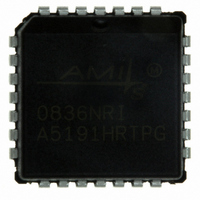
A5191HRTPG-XTD ON Semiconductor, A5191HRTPG-XTD Datasheet - Page 7

A5191HRTPG-XTD
Manufacturer Part Number
A5191HRTPG-XTD
Description
MODEM HART SGL CMOS 28-PLCC
Manufacturer
ON Semiconductor
Datasheet
1.A5191HRTPG-XTD.pdf
(14 pages)
Specifications of A5191HRTPG-XTD
Data Format
HART
Interface
CMOS
Voltage - Supply
3 V ~ 5.5 V
Mounting Type
Surface Mount
Package / Case
28-PLCC
Logic Type
CMOS Modem
Logic Family
A5191HRT
Input Level
CMOS
Supply Voltage (max)
5 V
Supply Voltage (min)
3.3 V
Maximum Operating Temperature
+ 85 C
Function
Use in highway addressable remote transducer (HART) field instruments and masters
Minimum Operating Temperature
- 40 C
Mounting Style
SMD/SMT
Supply Voltage Range
3V To 5.5V
Operating Temperature Range
-40°C To +85°C
Digital Ic Case Style
LCC
No. Of Pins
28
Msl
MSL 3 - 168 Hours
Filter Terminals
SMD
No. Of I/o's
1
Rohs Compliant
Yes
Communication Function
HART Modem
Lead Free Status / RoHS Status
Lead free / RoHS Compliant
Baud Rates
-
Lead Free Status / Rohs Status
Lead free / RoHS Compliant
Other names
766-1012
Available stocks
Company
Part Number
Manufacturer
Quantity
Price
Company:
Part Number:
A5191HRTPG-XTD
Manufacturer:
ON
Quantity:
37
Company:
Part Number:
A5191HRTPG-XTD
Manufacturer:
ON
Quantity:
3 211
Company:
Part Number:
A5191HRTPG-XTD
Manufacturer:
ON Semiconductor
Quantity:
10 000
Part Number:
A5191HRTPG-XTD
Manufacturer:
ON/安森美
Quantity:
20 000
Pin Descriptions
Table 8. PIN DESCRIPTIONS
AREF
CDREF
RESETB
RTSB
RxA
RxAFI
TxD
XIN
CBIAS
CD
RxAF
RxD
TxA
XOUT
TEST(12:1)
VDD
VDDA
VSS
VSSA
Symbol
Analog reference voltage
Carrier detect reference voltage
Reset digital logic
Request to send
Analog receive input
Analog receive comparator input
Digital transmit input
Oscillator input
Comparator bias current
Carrier detect output
Analog receive filter output
Digital receive output
Analog transmit output
Oscillator output
Factory test
Digital power
Analog supply voltage
Ground
Analog ground
Pin Name
Connection to the external bias resistor. R
AREF / R
Receiver Reference Voltage. Normally 1.23 V is selected (in combination with
VDDA = 3.3 V). See Table 2.
Carrier Detect Reference voltage. The value should be 85 mV below AREF to set
the carrier detection to a nominal of 100 mV
When at logic low (V
operation RESETB should be at V
of 10 nS after V
Active−low input selects the operation of the modulator. TxA is enabled when this
signal is low. This signal must be held high during power−up.
Receive Data Demodulator Input. Accepts a HART 1200 / 2200 Hz FSK modu-
lated square wave serial data stream as input.
Positive input of the carrier detect comparator and the receiver filter comparator.
Input to the modulator accepts digital data in NRZ form. When TxD is low, the
modulator output frequency is 2200 Hz. When TxD is high, the modulator output
frequency is 1200 Hz.
Input to the internal oscillator must be connected to a parallel mode 460.8 kHz
ceramic resonator when using the internal oscillator or grounded when using an
external 460.8 kHz clock signal.
Output goes high when a valid input is recognized on RxA. If the received signal
is greater than the threshold specified on CDREF for four cycles of the RxA sig-
nal, the valid input is recognized.
The output of the three pole high pass receive data filter
Signal outputs the digital receive data. When the received signal (RxA) is
1200 Hz, RxD outputs logic high. When the received signal (RxA) is 2200 Hz,
RxD outputs logic low. The HART receive data stream is only active if Carrier
Detect (CD) is high.
Transmit Data Modulator Output. A trapezoidal shaped waveform with a fre-
quency of 1200 Hz or 2200 Hz corresponding to a data value of 1 or 0 respect-
ively applied to TxD. TxA is active when RTSB is low. TxA equals 0.5 V when
RTSB is high.
Output from the internal oscillator must be connected to an external 460.8 kHz
clock signal or to a parallel mode 460.8 kHz ceramic resonator when using the
internal oscillator.
Factory test pins; for normal operation, tie these signals as per Tables 6 and 7
Power for the digital modem circuitry
Power for the analog modem circuitry
Digital ground (and Analog ground in the case of PLCC package)
Analog ground
http://onsemi.com
BIAS
7
= 2.5 mA ± 5 %
DD
= 2.5 V as shown in Figure 14.
SS
) this input holds all the digital logic in reset. During normal
DD
Description
. RESETB should be held low for a minimum
BIAS
p−p
should be selected such that
.


