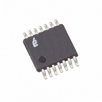
X96010V14IZ Intersil, X96010V14IZ Datasheet - Page 4

X96010V14IZ
Manufacturer Part Number
X96010V14IZ
Description
IC SENSOR CONDITIONER 14-TSSOP
Manufacturer
Intersil
Type
Sensor Conditionerr
Datasheet
1.X96010V14IZ.pdf
(26 pages)
Specifications of X96010V14IZ
Input Type
Voltage
Output Type
Voltage
Interface
2-Wire
Current - Supply
15mA
Mounting Type
Surface Mount
Package / Case
14-TSSOP
Lead Free Status / RoHS Status
Lead free / RoHS Compliant
Available stocks
Company
Part Number
Manufacturer
Quantity
Price
Company:
Part Number:
X96010V14IZ
Manufacturer:
IDT
Quantity:
989
Notes: 1. The device goes into Standby: 200 ns after any STOP, except those that initiate a nonvolatile write cycle. It goes into Standby t
ELECTRICAL CHARACTERISTICS
All typical values are for 25°C ambient temperature and 5V at pin Vcc. Maximum and minimum specifications are over
the recommended operating conditions. All voltages are referred to the voltage at pin Vss. Bit 3 in Control register 0 is
“1”, while all other bits in control registers are “0”. 255Ω, 0.1%, resistor connected between R1 and Vss, and another
between R2 and Vss. 400kHz TTL input at SCL. SDA pulled to Vcc through an external 2kΩ resistor. 2-wire interface
in “standby” (see notes 1 and 2 on page 5). WP, A0, A1, and A2 floating. VRef pin unloaded.
V
VRefout
RVref
TCOref
VRef Range
I
V
VccRamp
V
R
IHCMOS
POR
ADCOK
Symbol
2. t
3. For this range of V(VRef) the full scale sink mode current at I1 and I2 follows V(VRef) with a linearity error smaller than 1%.
4. This parameter is periodically sampled and not 100% tested.
5. TCO
a STOP that initiates a nonvolatile write cycle. It also goes into Standby 9 clock cycles after any START that is not followed by the cor-
rect Slave Address Byte.
is the minimum cycle time to be allowed for any nonvolatile write by the user, unless Acknowledge Polling is used.
WC
is the time from a valid STOP condition at the end of a write sequence to the end of the self-timed internal nonvolatile write cycle. It
ref
= [Max V(V
WP, A0, A1, and A2 input
High voltage
Output Voltage at VRef at
25°C
VRef pin input resistance
Temperature coefficient of
VRef output voltage
Voltage range when VRef
is an input
Current from pin R1 or R2
to Vss
Power-on reset threshold
voltage
Vcc Ramp Rate
ADC enable minimum
voltage
REF
Parameter
4
) - Min V(V
REF
(Continued)
)] x 10
6
/(1.21V x 140°C)
1.205
0.8 x
-100
Min
Vcc
1.5
0.2
2.6
20
(Conditions are as follows, unless otherwise specified)
1
0
X96010
1.21
Typ
1.215
+100
3200
Max
Vcc
1.3
2.8
2.8
40
50
ppm/°
Unit
mV /
kΩ
µA
µ
V
V
C
V
V
V
s
-20 µA ≤ I(VRef) ≤ 20 µA
VRM bit = “1”, 25°C
See note 4 and 5.
See note 3.
See Figure 10.
Test Conditions / Notes
October 25, 2005
WC
FN8214.1
after


