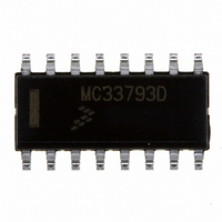
MC33793DR2 Freescale Semiconductor, MC33793DR2 Datasheet - Page 20

MC33793DR2
Manufacturer Part Number
MC33793DR2
Description
IC DSI SLAVE FOR R-SENSE 16-SOIC
Manufacturer
Freescale Semiconductor
Type
Distributed Systems Interfacer
Datasheet
1.MCZ33793EFR2.pdf
(27 pages)
Specifications of MC33793DR2
Input Type
Logic
Output Type
Logic
Interface
2 Line, I²C (CLK, Address/Data)
Mounting Type
Surface Mount
Package / Case
16-SOIC (3.9mm Width)
Lead Free Status / RoHS Status
Contains lead / RoHS non-compliant
Current - Supply
-
Lead Free Status / Rohs Status
Not Compliant
Other names
MC33793DR2TR
SET LOGIC OUT COMMAND
logic high. The compliment to this command is the Clear
Table 25. Set Logic Out Command Format
SET LOGIC OUT RESPONSE
following a valid Set Logic Out command to the addressed
Table 26. Set Logic Out Response Format
REVERSE INITIALIZATION
command and will only work under the condition that it has
not already been initialized. The command may be used
three ways. The first is to initialize a programmable address
device. The second is the first step in assigning a pre-
programmed address. The third is to initialize a pre-
programmed device.
with the NV bit set to zero. The command will be received by
the next daisy chain device with its bus switch open.
Reception of this command will assign the device address
and the group number. Reception of this command will also
cause the bus switch to close if BS = 1 and no fault is
detected.
20
33793
FUNCTIONAL DEVICE OPERATION
DSI COMMANDS AND RESPONSES
Legend
A[3:0] = Address bits. The address of the selected device.
Legend
A[3:0] - Address bits. The slave address.
BS = Bus Switch Position (1=closed)
IO[3:0] = Values at logic I/Os.
LO = Logic out driven level.
A3
The Set Logic Out command sets the Logic Out pin to a
This response message is sent during the next message
The Reverse Initialization is similar to the Initialization
For the first case this command is sent to address zero
-
A2
-
A1
-
High Byte
A0
-
Data
0
-
0
-
0
-
0
-
NV
A3
U
X[3:0] = Cyclic Redundancy Check (CRC). The CRC as calculated by the
master.
A2
Address
NV = Nonvolatile Memory Write. The value of the NV bit in the slave.
U = Undervoltage indicated true by a “1”.
X[3:0] = Cyclic Redundancy Check (CRC). The CRC as calculated by the
slave.
LO
A1
Logic Out. The Logic Out is cleared at power-up or following
a Clear command. The format of the Clear Logic Out
command is shown in
device. The response is shown in
generated if the command address field was $0.
same as the first except that the NV bit is set to one.
Reception of the command will assign the device address
and the group number and cause the bus switch to close if BS
= 1 and there are no faults. A Read/Write NVM command
then may be sent to complete the setting of a pre-
programmed address.
address in both PA3:PA0 and A3:A0 fields.
command, it will ignore further reverse initialization
commands or initialization commands unless it has received
a Clear command or undergone a power-up reset.
For the second case the Initialization command is sent the
A pre-programmed device must be initialized by putting its
Once a device has received a reverse initialization
The command format is found in
Low Byte
BS
A0
IO3
1
Command
IO2
1
Table
Analog Integrated Circuit Device Data
IO1
0
25.
IO0
1
Table
Freescale Semiconductor
Table
X3
X3
26. No response is
27.
X2
X2
CRC
CRC
X1
X1
X0
X0


