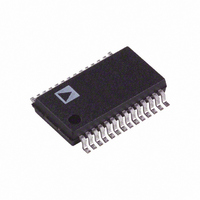
AD9822JRSZ Analog Devices Inc, AD9822JRSZ Datasheet - Page 15

AD9822JRSZ
Manufacturer Part Number
AD9822JRSZ
Description
IC CCD SIGNAL PROC 14BIT 28SSOP
Manufacturer
Analog Devices Inc
Type
CCD Signal Processor, 14-Bitr
Datasheet
1.AD9822JRSZRL.pdf
(20 pages)
Specifications of AD9822JRSZ
Input Type
Logic
Output Type
Logic
Interface
3-Wire Serial
Current - Supply
73mA
Mounting Type
Surface Mount
Package / Case
28-SSOP
Supply Voltage Range
3V To 5.25V, 4.75V To 5.25V
Power Dissipation Pd
450mW
Ic Mounting
SMD
Tv / Video Case Style
SSOP
No. Of Pins
28
Msl
MSL 3 - 168 Hours
Termination Type
SMD
Filter Terminals
SMD
Rohs Compliant
Yes
Digital Ic Case Style
SSOP
Lead Free Status / RoHS Status
Lead free / RoHS Compliant
Available stocks
Company
Part Number
Manufacturer
Quantity
Price
Company:
Part Number:
AD9822JRSZ
Manufacturer:
ADI
Quantity:
72
Part Number:
AD9822JRSZ
Manufacturer:
ADI/亚德诺
Quantity:
20 000
Part Number:
AD9822JRSZRL
Manufacturer:
ADI/亚德诺
Quantity:
20 000
CIRCUIT OPERATION
ANALOG INPUTS—CDS MODE
Figure 10 shows the analog input configuration for the CDS
mode of operation. Figure 11 shows the internal timing for the
sampling switches. The CCD reference level is sampled when
CDSCLK1 transitions from high to low, opening S1. The CCD
data level is sampled when CDSCLK2 transitions from high to
low, opening S2. S3 is then closed, generating a differential
output voltage representing the difference between the two
sampled levels.
The input clamp is controlled by CDSCLK1. When CDSCLK1 is
high, S4 closes and the internal bias voltage is connected to the
analog input. The bias voltage charges the external 0.1 µF input
capacitor, level-shifting the CCD signal into the AD9822’s input
common-mode range. The time constant of the input clamp is
determined by the internal 5 kΩ resistance and the external
0.1 µF input capacitance.
(INTERNAL)
Figure 10. CDS Mode Input Configuration (All Three Channels are Identical)
CDSCLK1
CDSCLK2
CCD SIGNAL
Q3
1µF
S1, S4 CLOSED
+
Figure 11. CDS Mode Internal Switch Timing
0.1µF
C
IN
OFFSET
S1, S4 OPEN
S2 OPEN
S3 OPEN
0.1µF
VINR
S2 CLOSED
AD9822
S4
S3 CLOSED
5kΩ
4V
3V
AVDD
S1, S4 CLOSED
1.7kΩ
2.2kΩ
6.9kΩ
S2
S1
INPUT CLAMP LEVEL
IS SELECTED IN THE
CONFIGURATION
REGISTER.
S3
S2 CLOSED
2pF
2pF
S3 CLOSED
CML
CML
Rev. B | Page 15 of 20
EXTERNAL INPUT COUPLING CAPACITORS
The recommended value for the input coupling capacitors is
0.1 µF. While it is possible to use a smaller capacitor, this larger
value is chosen for several reasons:
• Signal Attenuation: The input coupling capacitor creates a
• Linearity: Some of the input capacitance of a CMOS IC is
• Sampling Errors: The internal 2 pF sample capacitors have a
capacitive divider with a CMOS integrated circuit’s input
capacitance, attenuating the CCD signal level. CIN should be
large relative to the IC’s 10 pF input capacitance in order to
minimize this effect.
junction capacitance, which varies nonlinearly with applied
voltage. If the input coupling capacitor is too small, the
attenuation of the CCD signal varies nonlinearly with signal
level. This degrades the system linearity performance.
“memory” of the previously sampled pixel. There is a charge
redistribution error between CIN and the internal sample
capacitors for larger pixel-to-pixel voltage swings. As the
value of CIN is reduced, the resulting error in the sampled
voltage increases. With a CIN value of 0.1 µF, the charge
redistribution error is less than 1 LSB for a full-scale, pixel-to-
pixel voltage swing.
AD9822


