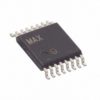
MXB7843EUE+T Maxim Integrated Products, MXB7843EUE+T Datasheet - Page 10

MXB7843EUE+T
Manufacturer Part Number
MXB7843EUE+T
Description
IC CNTRLR TOUCH RES 16TSSOP
Manufacturer
Maxim Integrated Products
Type
Resistiver
Datasheet
1.MXB7843EEE.pdf
(21 pages)
Specifications of MXB7843EUE+T
Touch Panel Interface
4-Wire
Number Of Inputs/keys
1 TSC
Resolution (bits)
12 b
Data Interface
MICROWIRE™, QSPI™, Serial, SPI™
Data Rate/sampling Rate (sps, Bps)
125k
Voltage Reference
External
Voltage - Supply
2.38 V ~ 5.25 V
Current - Supply
650µA
Operating Temperature
-40°C ~ 85°C
Mounting Type
Surface Mount
Package / Case
16-TSSOP
Output Type
Digital
Interface
4-Wire Serial
Input Type
Analog
Lead Free Status / RoHS Status
Lead free / RoHS Compliant
Internal protection diodes, which clamp the analog
input to V
swing from GND - 0.3V to V
Analog inputs must not exceed V
50mV or be lower than GND by more than 50mV for
accurate conversions. If an off-channel analog input
voltage exceeds the supplies, limit the input current to
50mA. The analog input pins are ESD protected to
±8kV using the Contact-Discharge method and ±15kV
using the Air-Gap method specified in IEC 61000-4-2.
The MXB7843 provides two conversion methods—dif-
ferential and single ended. The SER/DFR bit in the con-
trol word selects either mode. A logic 1 selects a
single-ended conversion, while a logic 0 selects a dif-
ferential conversion.
Changes in operating conditions can degrade the accu-
racy and repeatability of touch-screen measurements.
Therefore, the conversion results representing X and Y
coordinates may be incorrect. For example, in single-
ended measurement mode, variation in the touch-
screen driver voltage drops results in incorrect input
reading. Differential mode minimizes these errors.
Figure 3 shows the switching matrix configuration for
Y-coordinate measurement in single-ended mode. The
MXB7843 measures the position of the pointing device by
connecting X+ to IN+ of the ADC, enabling Y+ and Y- dri-
vers, and digitizing the voltage on X+. The ADC performs
a conversion with REF+ = REF and REF- = GND. In sin-
gle-ended measurement mode, the bias to the touch
screen can be turned off after the acquisition to save
power. The on-resistance of the X and Y drivers results in
a gain error in single-ended measurement mode. Touch-
screen resistance ranges from 200Ω to 900Ω (depending
on the manufacturer), whereas the on-resistance of the X
and Y drivers is 8Ω (typ). Limit the touch-screen current to
less than 50mA by using a touch screen with a resistance
higher than 100Ω. The resistive divider created by the
touch screen and the on-resistance of the X and Y drivers
result in both an offset and a gain shift. Also, the on-resis-
tance of the X and Y drivers does not track the resistance
of the touch screen over temperature and supply. This
results in further measurement errors.
2.375V to 5.25V, 4-Wire Touch-Screen
Controller
10
______________________________________________________________________________________
DD
and GND, allow the analog input pins to
Touch-Screen Conversion
Analog Input Protection
Differential vs. Single Ended
DD
+ 0.3V without damage.
Single-Ended Mode
DD
by more than
Figure 4 shows the switching matrix configuration for
Y-coordinate measurement. The REF+ and REF- inputs
are connected directly to the Y+ and Y- pins, respec-
tively. Differential mode uses the voltage at the Y+ pin
as the REF+ voltage and voltage at the Y- pin as REF-
voltage. This conversion is ratiometric and independent
of the voltage drop across the drivers and variation in
the touch-screen resistance. In differential mode, the
touch screen remains biased during the acquisition and
conversion process. This results in additional supply
current and power dissipation during conversion when
compared to the absolute measurement mode.
Figure 5 shows the block diagram for the PENIRQ func-
tion. When used, PENIRQ requires a 10kΩ to 100kΩ
pullup to +V
the touch screen is touched. The PENIRQ output can
be used to initiate an interrupt to the microprocessor,
which can write a control word to the MXB7843 to start
a conversion.
Figure 6 shows the timing diagram for the PENIRQ pin
function. The diagram shows that once the screen is
touched while CS is high, the PENIRQ output goes low
after a time period indicated by t
value changes for different touch-screen parasitic
capacitance and resistance. The microprocessor
receives this interrupt and pulls CS low to initiate a con-
version. At this instant, the PENIRQ pin should be
masked, as transitions can occur due to a selected
input channel or the conversion mode. The PENIRQ pin
functionality becomes valid when either the last data bit
is clocked out, or CS is pulled high.
During conversion, an external reference at REF must
deliver up to 40µA DC load current. If the reference has
a higher output impedance or is noisy, bypass it close
to the REF pin with a 0.1µF and a 4.7µF capacitor.
DD
. If enabled, PENIRQ goes low whenever
PEN Interrupt Request (
Differential Measurement Mode
External Reference
TOUCH
. The t
PENIRQ )
TOUCH


