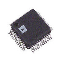
AD9845AJST Analog Devices Inc, AD9845AJST Datasheet - Page 3

AD9845AJST
Manufacturer Part Number
AD9845AJST
Description
IC CCD SIGNAL PROC 12BIT 48-LQFP
Manufacturer
Analog Devices Inc
Type
CCD Signal Processor, 12-Bitr
Datasheet
1.AD9845AJST.pdf
(22 pages)
Specifications of AD9845AJST
Rohs Status
RoHS non-compliant
Input Type
Logic
Output Type
Logic
Interface
3-Wire Serial
Mounting Type
Surface Mount
Package / Case
48-LQFP
Current - Supply
-
Lead Free Status / RoHS Status
Not Compliant
Available stocks
Company
Part Number
Manufacturer
Quantity
Price
Part Number:
AD9845AJST
Manufacturer:
AD
Quantity:
20 000
CCD-MODE SPECIFICATIONS
Parameter
P
MAXIMUM CLOCK RATE
CDS
PIXEL GAIN AMPLIFIER (PxGA)
VARIABLE GAIN AMPLIFIER (VGA)
BLACK LEVEL CLAMP
SYSTEM PERFORMANCE
POWER-UP RECOVERY TIME
NOTES
1
2
Specifications subject to change without notice.
RESET TRANSIENT
Input Signal Characteristics defined as follows:
PxGA gain fixed at 4 dB (Code 63).
OWER CONSUMPTION
Gain
Allowable CCD Reset Transient
Max Input Range Before Saturation
Max CCD Black Pixel Amplitude
Max Input Range
Max Output Range
Gain Control Resolution
Gain Monotonicity
Gain Range (Two’s Complement Coding)
Max Input Range
Max Output Range
Gain Control Resolution
Gain Monotonicity
Gain Range
Clamp Level Resolution
Clamp Level
Gain Accuracy (VGA Code 91 to 1023)
PxGA Gain Accuracy
Peak Nonlinearity, 500 mV Input Signal
Total Output Noise
Power Supply Rejection (PSR)
Fast Recovery Mode
Reference Standby Mode
Total Shutdown Mode
Power-Off Condition
500mV TYP
Min Gain (PxGA Gain Code 32)
Max Gain (PxGA Gain Code 31)
Low Gain (VGA Gain Code 91)
Max Gain (VGA Gain Code 1023)
Min Clamp Level
Max Clamp Level
Min Gain (PxGA Register Code 32)
Max Gain (PxGA Code 31)
OPTICAL BLACK PIXEL
200mV MAX
INPUT SIGNAL RANGE
1V MAX
1
1
1
2
(T
Min
30
1.0
1.0
1.6
1.6
2.0
–0.5
–1
11
MIN
to T
MAX
Guaranteed
Guaranteed
Typ
140
0
500
200
64
–2
10
1024
2
36
256
0
255
0
12
0.1
0.6
40
0.1
1
3
15
, AVDD = DVDD = 3.0 V, f
Max
+0.5
+1
13
mV
V p-p
V p-p
V p-p
dB
dB
%
LSB rms
dB
ms
Unit
mW
MHz
dB
mV
V p-p
Steps
dB
dB
V p-p
Steps
dB
dB
Steps
LSB
LSB
ms
ms
ms
DATACLK
= f
SHP
Notes
See TPC 1 for Power Curves
See Input Waveform in Footnote 1
PxGA Gain at 4 dB
See Figure 28 for PxGA Gain Curve
See Figure 29 for VGA Gain Curve
Measured at ADC Output
Specifications Include Entire Signal Chain
Use Equations on Page 18 to Calculate Gain
VGA Gain Fixed at 2 dB (Code 91)
VGA Gain Fixed at 2 dB (Code 91)
12 dB Gain Applied
AC Grounded Input, 6 dB Gain Applied
Measured with Step Change on Supply
Normal Clock Signals Applied
= f
SHD
= 30 MHz, unless otherwise noted.)
AD9845A


