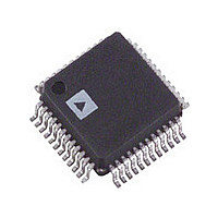
AD9847AKST Analog Devices Inc, AD9847AKST Datasheet - Page 10

AD9847AKST
Manufacturer Part Number
AD9847AKST
Description
IC CCD SIGNAL PROC 10BIT 48-LQFP
Manufacturer
Analog Devices Inc
Type
CCD Signal Processor, 10-Bitr
Datasheet
1.AD9847AKSTZRL.pdf
(28 pages)
Specifications of AD9847AKST
Rohs Status
RoHS non-compliant
Input Type
Logic
Output Type
Logic
Interface
3-Wire Serial
Mounting Type
Surface Mount
Package / Case
48-LQFP
Analog Front End Type
CCD
Analog Front End Category
Video
Interface Type
Serial (3-Wire)
Sample Rate
40MSPS
Input Voltage Range
0.5V
Operating Supply Voltage (min)
2.7/3V
Operating Supply Voltage (typ)
3.3/5V
Operating Supply Voltage (max)
3.6/5.5V
Resolution
10b
Number Of Adc's
1
Power Supply Type
Analog/Digital
Operating Temp Range
-20C to 85C
Operating Temperature Classification
Commercial
Mounting
Surface Mount
Pin Count
48
Package Type
LQFP
Number Of Channels
1
Current - Supply
-
Lead Free Status / RoHS Status
Not Compliant
Available stocks
Company
Part Number
Manufacturer
Quantity
Price
Company:
Part Number:
AD9847AKST
Manufacturer:
AD
Quantity:
1 831
Company:
Part Number:
AD9847AKST
Manufacturer:
ADI
Quantity:
244
Part Number:
AD9847AKST
Manufacturer:
ADI/亚德诺
Quantity:
20 000
Company:
Part Number:
AD9847AKSTZ
Manufacturer:
Analog Devices Inc
Quantity:
10 000
Company:
Part Number:
AD9847AKSTZRL
Manufacturer:
Analog Devices Inc
Quantity:
10 000
AD9847
Accessing a Double-Wide Register
There are many double-wide registers in the AD9847, e.g.,
oprmode, clpdmtog1_0, and clpdmscp3, and so on. These regis-
ters are configured into two consecutive 6-bit registers with the
least significant six bits located in the lower of the two addresses
and the remaining most significant bits located in the higher of
the two addresses. For example, the six LSBs of the clpdmscp3
register, clpdmscp3[5:0], are located at address 0x81. The most
significant six bits of the clpdmscp3 register, clpdmscp3[11:6],
are located at Address 0x82. The following rules must be fol-
lowed when accessing double-wide registers:
1. When accessing a double-wide register, BOTH addresses
2. The lower of the two consecutive addresses for the double-
Address
AFE Registers # Bits 56
00
01
02
03
04
05
06
07
08
09
0A
Miscellaneous/Extra # Bits 26
0F
16
17
18
19
1B
1C
1D
1E
1F
20
26
must be written to.
wide register must be written to first. In the example of the
Bit
Content
[5:0]
[1:0]
[5:0]
[3:0]
[5:0]
[1:0]
[5:0]
[5:0]
[5:0]
[5:0]
[5:0]
[5:0]
[0]
[5:0]
[5:0]
[0]
[5:0]
[0]
[0]
[0]
[0]
[5:0]
[0]
Width
6
2
6
4
6
2
6
6
6
6
6
6
1
6
6
1
6
1
1
1
1
6
1
Default
Value
00
00
16
02
00
02
00
00
00
00
00
00
00
00
00
00
00
00
00
01
00
00
00
ctlmode
pxga gain0
pxga gain1
pxga gain2
pxga gain3
update[5:0]
update[11:6]
vdhdpol
hblkretime
Register Name
oprmode[5:0]
oprmode[7:6]
ccdgain[5:0]
ccdgain[9:6]
refblack[5:0]
refblack[7:6]
INITIAL2
out_cont
preventupdate
doutphase
disablerestore
fieldval
INITIAL1
tgcore_rstb
–10–
3. A single write to the lower of the two consecutive addresses
4. A single write to the higher of the two consecutive addresses of a
clpdmscp3 register, the contents of Address 0x81 must be
written first, followed by the contents of Address 0x82. The
register will be updated after the completion of the write to
Register 0x82, either at the next SL rising edge or the next
VD/HD falling edge.
of a double-wide register that is not followed by a write to the
higher address of the registers is not permitted. This will not
update the register.
double-wide register that is not preceded by a write to the lower
of the two addresses is not permitted. Although the write to the
higher address will update the full double-wide register, the
lower six bits of the register will be written with an indetermi-
nate value if the lower address was not written to first.
Register Description
AFE Operation Mode (See AFE Register Breakdown)
VGA Gain
Black Clamp Level
Control Mode (See AFE Register Breakdown)
PxGA Color 0 Gain
PxGA Color 1 Gain
PxGA Color 2 Gain
PxGA Color 3 Gain
See Recommended Power Up Sequence Section. Should be
set to “4” decimal (000100).
Output Control (0 = Make All Outputs DC Inactive)
Serial Data Update Control (Sets the line within the field
for serial data update to occur)
Prevent the Update of the VD/HD Updated Registers
DOUT Phase Control
Disable CCDIN DC Restore Circuit During PBLK
(1 = Disable)
VD/HD Active Polarity (0 = Low Active, 1 = High Active)
Internal Field Pulse Value (0 = Next Field Odd,
1 = Next Field Even)
Re-Sync hblk to h1 Clock
See Recommended Power Up Sequence. Should be set to
“53” decimal (110101).
TG Core Reset_Bar (0 = Hold TG Core in Reset,
1 = Resume Normal Operation)
REV. A


