DS92LV1212AMSA/NOPB National Semiconductor, DS92LV1212AMSA/NOPB Datasheet - Page 2
DS92LV1212AMSA/NOPB
Manufacturer Part Number
DS92LV1212AMSA/NOPB
Description
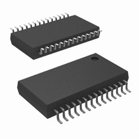
IC DESERIALIZER 10-BIT 28-SSOP
Manufacturer
National Semiconductor
Datasheet
1.DS92LV1212AMSANOPB.pdf
(15 pages)
Specifications of DS92LV1212AMSA/NOPB
Function
Deserializer
Data Rate
400Mbps
Input Type
LVDS
Output Type
LVDS
Number Of Inputs
1
Number Of Outputs
10
Voltage - Supply
3 V ~ 3.6 V
Operating Temperature
-40°C ~ 85°C
Mounting Type
Surface Mount
Package / Case
28-SSOP
Lead Free Status / RoHS Status
Lead free / RoHS Compliant
Other names
*DS92LV1212AMSA
*DS92LV1212AMSA/NOPB
DS92LV1212AMSA
*DS92LV1212AMSA/NOPB
DS92LV1212AMSA
Available stocks
Company
Part Number
Manufacturer
Quantity
Price
Company:

Part Number:
DS92LV1212AMSA/NOPB
Manufacturer:
TI
Quantity:
1 900


www.national.com
Block Diagram
Functional Description
The DS92LV1212 is a 10-bit Deserializer chip designed to
receive data over heavily loaded differential backplanes at
clock speeds from 16 MHz to 40 MHz. It may also be used to
receive data over Unshielded Twisted Pair (UTP) cable.
The chip has three active states of operation: Initialization,
Data Transfer, and Resynchronization; and two passive
states: Powerdown and TRI-STATE
The following sections describe each operation of the active
and passive states.
Initialization
Before data can be transferred, the Deserializer must be
initialized. The Deserializer should be powered up with the
PWRDN pin held low. After V
can be forced high. The Deserializer is ready to lock to the
incoming data stream.
Step 1: When you apply V
tive outputs are held in TRI-STATE and internal circuitry is
disabled by on-chip power-on circuitry. When V
V
synchronization patterns. You must apply the local clock to
the REFCLK pin.
The Deserializer LOCK output will remain high while its PLL
locks to incoming data or to SYNC patterns on the inputs.
Step 2: The Deserializer PLL must synchronize to the Seri-
alizer to complete the initialization. The Deserializer will lock
to non-repetitive data patterns; however, the transmission of
SYNC patterns to the Deserializer enables the Deserializer
to lock to the Serializer signal within a specified time. See
Figure 7 .
The user’s application determines control of the SYNC1 and
SYNC2 pins. One recommendation is a direct feedback loop
from the LOCK pin. Under all circumstances, the Serializer
stops sending SYNC patterns after both SYNC inputs return
low.
When the Deserializer detects edge transitions at the Bus
LVDS input, it will attempt to lock to the embedded clock
information. When the Deserializer locks to the Bus LVDS
clock, the LOCK output will go low. When LOCK is low, the
Deserializer outputs represent incoming Bus LVDS data.
CC
OK (2.5V), the PLL is ready to lock to incoming data or
CC
(Continued)
to the Deserializer, the respec-
CC
stabilizes, the PWRDN pin
®
.
CC
reaches
Application
2
Data Transfer
After initialization, the Serializer will accept data from inputs
DIN0–DIN9. The Serializer uses the TCLK input to latch
incoming Data. The TCLK_R/F pin selects which edge the
Serializer uses to strobe incoming data. TCLK_R/F high
selects the rising edge for clocking data and low selects the
falling edge. If either of the SYNC inputs is high for 5*TCLK
cycles, the data at DIN0-DIN9 is ignored regardless of clock
edge.
After determining which clock edge to use, a start and stop
bit, appended internally, frame the data bits in the register.
The start bit is always high and the stop bit is always low.
The start and stop bits function as the embedded clock bits
in the serial stream.
Serialized data and clock bits (10+2 bits) are received at 12
times the TCLK frequency. For example, if TCLK is 40 MHz,
the serial rate is 40 x 12 = 480 Mega bits per second. Since
only 10 bits are from input data, the serial “payload” rate is
10 times the TCLK frequency. For instance, if TCLK = 40
MHz, the payload data rate is 40 x 10 = 400 Mbps. TCLK is
provided by the data source and must be in the range 16
MHz to 40 MHz nominal.
The LOCK pin on the Deserializer is driven low when it is
synchronized with the Serializer. The Deserializer locks to
the embedded clock and uses it to recover the serialized
data. ROUT data is valid when LOCK is low. Otherwise,
ROUT0–ROUT9 is invalid.
The ROUT0-ROUT9 pins use the RCLK pin as the reference
to data. The polarity of the RCLK edge is controlled by the
RCLK_R/F input. See Figure 5 .
ROUT(0-9), LOCK and RCLK outputs will drive a minimum
of three CMOS input gates (15 pF load) with 40 MHz clock.
Resynchronization
When the Deserializer PLL locks to the embedded clock
edge, the Deserializer LOCK pin asserts a low. If the Dese-
rializer loses lock, the LOCK pin output will go high and the
outputs (including RCLK) will enter TRI-STATE.
The user’s system monitors the LOCK pin to detect a loss of
synchronization. Upon detection, the system can arrange to
pulse the Serializer SYNC1 or SYNC2 pin to resynchronize.
Multiple resynchronization approaches are possible. One
DS101387-2
Related parts for DS92LV1212AMSA/NOPB
Image
Part Number
Description
Manufacturer
Datasheet
Request
R

Part Number:
Description:
16-40 Mhz 10-bit Bus Lvds Random Lock Deserializer With Embedded Clock Recovery
Manufacturer:
National Semiconductor Corporation
Datasheet:

Part Number:
Description:
National Semiconductor [8-Bit D/A Converter]
Manufacturer:
National Semiconductor
Datasheet:
Part Number:
Description:
National Semiconductor [Media Coprocessor]
Manufacturer:
National Semiconductor
Datasheet:
Part Number:
Description:
Digitally Controlled Tone and Volume Circuit with Stereo Audio Power Amplifier, Microphone Preamp Stage and National 3D Sound
Manufacturer:
National Semiconductor
Datasheet:
Part Number:
Description:
Digitally Controlled Tone and Volume Circuit with Stereo Audio Power Amplifier, Microphone Preamp Stage and National 3D Sound
Manufacturer:
National Semiconductor
Datasheet:
Part Number:
Description:
AC97 Rev 2 Codec with Sample Rate Conversion and National 3D Sound
Manufacturer:
National Semiconductor
Part Number:
Description:
Manufacturer:
National Semiconductor
Datasheet:
Part Number:
Description:
Manufacturer:
National Semiconductor
Datasheet:
Part Number:
Description:
General Purpose, Low Voltage, Low Power, Rail-to-Rail Output Operational Amplifiers
Manufacturer:
National Semiconductor
Datasheet:
Part Number:
Description:
8-bit 20 MSPS flash A/D converter.
Manufacturer:
National Semiconductor
Datasheet:
Part Number:
Description:
Low Noise Quad Operational Amplifier
Manufacturer:
National Semiconductor
Datasheet:
Part Number:
Description:
Quad Differential Line Receivers
Manufacturer:
National Semiconductor
Datasheet:
Part Number:
Description:
Quad High Speed Trapezoidal? Bus Transceiver
Manufacturer:
National Semiconductor
Datasheet:
Part Number:
Description:
Dual Line Receiver
Manufacturer:
National Semiconductor
Datasheet: