DS92LV1023EMQ/NOPB National Semiconductor, DS92LV1023EMQ/NOPB Datasheet - Page 2
DS92LV1023EMQ/NOPB
Manufacturer Part Number
DS92LV1023EMQ/NOPB
Description
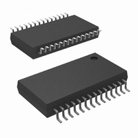
IC SERIALIZER 10-BIT 28-SSOP
Manufacturer
National Semiconductor
Datasheet
1.DS92LV1023EMQNOPB.pdf
(13 pages)
Specifications of DS92LV1023EMQ/NOPB
Function
Serializer
Data Rate
660Mbps
Input Type
LVTTL/LVCMOS
Output Type
LVDS
Number Of Inputs
10
Number Of Outputs
1
Voltage - Supply
3 V ~ 3.6 V
Operating Temperature
-40°C ~ 85°C
Mounting Type
Surface Mount
Package / Case
28-SSOP
Lead Free Status / RoHS Status
Lead free / RoHS Compliant
Other names
*DS92LV1023EMQ/NOPB
DS92LV1023EMQ
DS92LV1023EMQ
Available stocks
Company
Part Number
Manufacturer
Quantity
Price
Company:

Part Number:
DS92LV1023EMQ/NOPB
Manufacturer:
Maxim
Quantity:
313


www.national.com
Block Diagrams
Functional Description
The DS92LV1023E is a 10-bit Serializer device which to-
gether with a compatible deserializer (i.e. DS92LV1224)
forms a chipset designed to transmit data over FR-4 printed
circuit board backplanes and balanced copper cables at
clock speeds from 30 to 66 MHz.
The chipset has three active states of operation: Initializa-
tion, Data Transfer, and Resynchronization; and two passive
states: Powerdown and TRI-STATE
The following sections describe each operation and passive
state.
Initialization
Initialization of both devices must occur before data trans-
mission begins. Initialization refers to synchronization of the
Serializer and Deserializer PLL’s to local clocks, which may
be the same or separate. Afterwards, synchronization of the
Deserializer to Serializer occurs.
Step 1: When you apply V
rializer, the respective outputs enter TRI-STATE
chip power-on circuitry disables internal circuitry. When V
reaches V
ing to a local clock. For the Serializer, the local clock is the
transmit clock (TCLK) provided by the source ASIC or other
device. For the Deserializer, you must apply a local clock to
the REFCLK pin.
The Serializer outputs remain in TRI-STATE while the PLL
locks to the TCLK. After locking to TCLK, the Serializer is
now ready to send data or SYNC patterns, depending on the
levels of the SYNC1 and SYNC2 inputs or a data stream.
The SYNC pattern sent by the Serializer consists of six ones
and six zeros switching at the input clock rate.
Note that the Deserializer LOCK output will remain high
while its PLL locks to the incoming data or to SYNC patterns
on the input.
Step 2: The Deserializer PLL must synchronize to the Seri-
alizer to complete initialization. The Deserializer will lock to
non-repetitive data patterns. However, the transmission of
SYNC patterns enables the Deserializer to lock to the Seri-
alizer signal within a specified time. See Figure 7.
CC
OK (2.5V) the PLL in each device begins lock-
CC
to both Serializer and/or Dese-
(Continued)
®
.
®
, and on-
CC
Application
2
The user’s application determines control of the SYNC1 and
SYNC 2 pins. One recommendation is a direct feedback loop
from the LOCK pin. Under all circumstances, the Serializer
stops sending SYNC patterns after both SYNC inputs return
low.
When the Deserializer detects edge transitions at the Bus
LVDS input, it will attempt to lock to the embedded clock
information. When the Deserializer locks to the Bus LVDS
clock, the LOCK output will go low. When LOCK is low, the
Deserializer outputs represent incoming Bus LVDS data.
Data Transfer
After initialization, the Serializer will accept data from inputs
DIN0–DIN9. The Serializer uses the TCLK input to latch
incoming Data. The TCLK_R/F pin selects which edge the
Serializer uses to strobe incoming data. TCLK_R/F high
selects the rising edge for clocking data and low selects the
falling edge. If either of the SYNC inputs is high for 5*TCLK
cycles, the data at DIN0-DIN9 is ignored regardless of clock
edge.
After determining which clock edge to use, a start and stop
bit, appended internally, frame the data bits in the register.
The start bit is always high and the stop bit is always low.
The start and stop bits function as the embedded clock bits
in the serial stream.
The Serializer transmits serialized data and clock bits (10+2
bits) from the serial data output (DO
frequency. For example, if TCLK is 66 MHz, the serial rate is
66 x 12 = 792 Mega-bits-per-second. Since only 10 bits are
from input data, the serial “payload” rate is 10 times the
TCLK frequency. For instance, if TCLK = 66 MHz, the pay-
load data rate is 66 x 10 = 660 Mbps. The data source
provides TCLK and must be in the range of 30 MHz to 66
MHz nominal.
The Serializer outputs (DO
nection or in limited multi-point or multi-drop backplanes.
The outputs transmit data when the enable pin (DEN) is
high, PWRDN = high, and SYNC1 and SYNC2 are low.
When DEN is driven low, the Serializer output pins will enter
TRI-STATE.
When the Deserializer synchronizes to the Serializer, the
LOCK pin is low. The Deserializer locks to the embedded
±
) can drive a point-to-point con-
±
) at 12 times the TCLK
20131802
Related parts for DS92LV1023EMQ/NOPB
Image
Part Number
Description
Manufacturer
Datasheet
Request
R

Part Number:
Description:
Manufacturer:
National Semiconductor
Datasheet:
Part Number:
Description:
National Semiconductor [8-Bit D/A Converter]
Manufacturer:
National Semiconductor
Datasheet:
Part Number:
Description:
National Semiconductor [Media Coprocessor]
Manufacturer:
National Semiconductor
Datasheet:
Part Number:
Description:
Digitally Controlled Tone and Volume Circuit with Stereo Audio Power Amplifier, Microphone Preamp Stage and National 3D Sound
Manufacturer:
National Semiconductor
Datasheet:
Part Number:
Description:
Digitally Controlled Tone and Volume Circuit with Stereo Audio Power Amplifier, Microphone Preamp Stage and National 3D Sound
Manufacturer:
National Semiconductor
Datasheet:
Part Number:
Description:
AC97 Rev 2 Codec with Sample Rate Conversion and National 3D Sound
Manufacturer:
National Semiconductor
Part Number:
Description:
Manufacturer:
National Semiconductor
Datasheet:
Part Number:
Description:
Manufacturer:
National Semiconductor
Datasheet:
Part Number:
Description:
General Purpose, Low Voltage, Low Power, Rail-to-Rail Output Operational Amplifiers
Manufacturer:
National Semiconductor
Datasheet:
Part Number:
Description:
8-bit 20 MSPS flash A/D converter.
Manufacturer:
National Semiconductor
Datasheet:
Part Number:
Description:
Low Noise Quad Operational Amplifier
Manufacturer:
National Semiconductor
Datasheet:
Part Number:
Description:
Quad Differential Line Receivers
Manufacturer:
National Semiconductor
Datasheet:
Part Number:
Description:
Quad High Speed Trapezoidal? Bus Transceiver
Manufacturer:
National Semiconductor
Datasheet:
Part Number:
Description:
Dual Line Receiver
Manufacturer:
National Semiconductor
Datasheet: