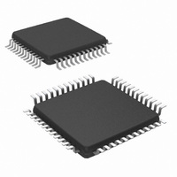
DS99R104TVS/NOPB National Semiconductor, DS99R104TVS/NOPB Datasheet - Page 12

DS99R104TVS/NOPB
Manufacturer Part Number
DS99R104TVS/NOPB
Description
IC DESERIALIZ 40MHZ 24BIT 48TQFP
Manufacturer
National Semiconductor
Datasheet
1.DS99R103TSQNOPB.pdf
(24 pages)
Specifications of DS99R104TVS/NOPB
Function
Deserializer
Data Rate
960Mbps
Input Type
LVTTL/LVCMOS
Output Type
LVDS
Number Of Inputs
1
Number Of Outputs
24
Voltage - Supply
3 V ~ 3.6 V
Operating Temperature
-40°C ~ 85°C
Mounting Type
Surface Mount
Package / Case
48-TQFP, 48-VQFP
Lead Free Status / RoHS Status
Lead free / RoHS Compliant
Other names
DS99R104TVS
Available stocks
Company
Part Number
Manufacturer
Quantity
Price
Company:
Part Number:
DS99R104TVS/NOPB
Manufacturer:
NSC
Quantity:
355
Company:
Part Number:
DS99R104TVS/NOPB
Manufacturer:
Texas Instruments
Quantity:
10 000
www.national.com
LVCMOS PARALLEL INTERFACE PINS
4-1,
48-44,
41-32,
29-25
10
CONTROL AND CONFIGURATION PINS
9
18
23
11
12
5
8
13
LVDS SERIAL INTERFACE PINS
20
19
POWER / GROUND PINS
22
21
16
17
14
15
30
31
7
6
42
43
24
Pin #
DS99R103 Serializer Pin Descriptions
DIN[23:0]
TCLK
TPWDNB
DEN
PRE
TRFB
VODSEL
DCAOFF
DCBOFF
RESRVD
DOUT+
DOUT−
VDDDR
VSSDR
VDDPT0
VSSPT0
VDDPT1
VSSPT1
VDDT
VSST
VDDL
VSSL
VDDIT
VSSIT
VSS
Pin Name
LVCMOS_I
LVCMOS_I
LVCMOS_I
LVCMOS_I
LVCMOS_I
LVCMOS_I
LVCMOS_I
LVCMOS_I
LVCMOS_I
LVCMOS_I
LVDS_O
LVDS_O
VDD
GND
VDD
GND
VDD
GND
VDD
GND
VDD
GND
VDD
GND
GND
I/O
Transmitter Parallel Interface Data Inputs Pins. Tie LOW if unused, do not float.
Transmitter Parallel Interface Clock Input Pin. Strobe edge set by TRFB configuration pin
Transmitter Power Down Bar
TPWDNB = H; Transmitter is Enabled and ON
TPWDNB = L; Transmitter is in power down mode (Sleep), LVDS Driver DOUT (+/-) Outputs
are in TRI-STATE stand-by mode, PLL is shutdown to minimize power consumption.
Transmitter Data Enable
DEN = H; LVDS Driver Outputs are Enabled (ON).
DEN = L; LVDS Driver Outputs are Disabled (OFF), Transmitter LVDS Driver DOUT (+/-)
Outputs are in TRI-STATE, PLL still operational and locked to TCLK.
PRE-emphasis select pin.
PRE = (R
PRE = No Connect (NC); pre-emphasis is disabled
Transmitter Clock Edge Select Pin
TRFB = H; Parallel Interface Data is strobed on the Rising Clock Edge.
TRFB = L; Parallel Interface Data is strobed on the Falling Clock Edge
VOD Level Select
VODSEL = L; LVDS Driver Output is
VODSEL = H; LVDS Driver Output is
For normal applications, set this pin LOW. For long cable applications where a larger VOD is
required, set this pin HIGH.
RESERVED – This pin MUST be tied LOW.
RESERVED – This pin MUST be tied LOW.
RESERVED – This pin MUST be tied LOW.
Transmitter LVDS True (+) Output. This output is intended to be loaded with a 100 ohm load to
the DOUT+ pin. The interconnect should be AC Coupled to this pin with a 100 nF capacitor.
Transmitter LVDS Inverted (-) Output This output is intended to be loaded with a 100 ohm load
to the DOUT- pin. The interconnect should be AC Coupled to this pin with a 100 nF capacitor.
Analog Voltage Supply, LVDS Output Power
Analog Ground, LVDS Output Ground
Analog Voltage supply, VCO Power
Analog Ground, VCO Ground
Analog Voltage supply, PLL Power
Analog Ground, PLL Ground
Digital Voltage supply, Tx Serializer Power
Digital Ground, Tx Serializer Ground
Digital Voltage supply, Tx Logic Power
Digital Ground, Tx Logic Ground
Digital Voltage supply, Tx Input Power
Digital Ground, Tx Input Ground
ESD Ground
PRE
≥
3 kΩ); I
max
12
= [(1.2/R)*20], R
≈
≈
±400 mV (R
±750 mV (R
Description
min
= 3 kΩ
L
L
= 100Ω)
= 100Ω)


