DS92LV18TVV/NOPB National Semiconductor, DS92LV18TVV/NOPB Datasheet - Page 2
DS92LV18TVV/NOPB
Manufacturer Part Number
DS92LV18TVV/NOPB
Description
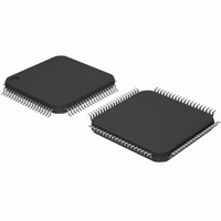
IC SER/DES LVDS 18BIT BUS 80LQFP
Manufacturer
National Semiconductor
Datasheet
1.DS92LV18TVVNOPB.pdf
(20 pages)
Specifications of DS92LV18TVV/NOPB
Function
Serializer/Deserializer
Data Rate
2.38Gbps
Input Type
LVTTL/LVCMOS
Output Type
LVTTL, LVCMOS
Number Of Inputs
18
Number Of Outputs
1
Voltage - Supply
3.15 V ~ 3.45 V
Operating Temperature
-40°C ~ 85°C
Mounting Type
Surface Mount
Package / Case
80-LQFP
No. Of Inputs
18
No. Of Outputs
18
Supply Voltage Range
3.15V To 3.45V
Driver Case Style
LQFP
No. Of Pins
80
Msl
MSL 3 - 168 Hours
Termination Type
SMD
Rohs Compliant
Yes
Filter Terminals
SMD
Digital Ic Case Style
LQFP
For Use With
LVDS-18B-EVK - BOARD EVALUATION DS92LV18
Lead Free Status / RoHS Status
Lead free / RoHS Compliant
Other names
*DS92LV18TVV
*DS92LV18TVV/NOPB
DS92LV18TVV
*DS92LV18TVV/NOPB
DS92LV18TVV
Available stocks
Company
Part Number
Manufacturer
Quantity
Price
Company:

Part Number:
DS92LV18TVV/NOPB
Manufacturer:
TI
Quantity:
1 000
Company:
Part Number:
DS92LV18TVV/NOPB
Manufacturer:
TI
Quantity:
2 170
Company:
Part Number:
DS92LV18TVV/NOPB
Manufacturer:
Texas Instruments
Quantity:
10 000
Part Number:
DS92LV18TVV/NOPB
Manufacturer:
NS/国半
Quantity:
20 000


www.national.com
LVCMOS/LVTTL DC Specifications
Bus LVDS DC specifications
Symbol
Absolute Maximum Ratings
If Military/Aerospace specified devices are required,
please contact the National Semiconductor Sales Office/
Distributors for availability and specifications.
Electrical Characteristics
Over recommended operating supply and temperature ranges unless otherwise specified.
VTH
V
VTL
V
V
V
I
I
V
I
I
OS
OZ
IN
OH
IN
OL
CL
IH
IL
Supply Voltage (V
LVCMOS/LVTTL Input
Voltage
LVCMOS/LVTTL Output
Voltage
Bus LVDS Receiver Input
Voltage
Bus LVDS Driver Output
Voltage
Bus LVDS Output Short
Circuit
Junction Temperature
Storage Temperature
Lead Temperature
(Soldering, 4 seconds)
TRI-STATETRI-STATE
Output Short Circuit Current
Differential Threshold High
High Level Output Voltage
Low Level Output Voltage
Differential Threshold Low
Duration
High Level Input Voltage
Low Level Input Voltage
Input Clamp Voltage
Input Current
Input Current
Parameter
CC
Current
Voltage
Voltage
)
−0.3V to (V
−0.3V to (V
®
Output
−65˚C to +150˚C
−0.3V to +3.9V
−0.3V to +3.9V
−0.3V to +4V
V
CC
CC
0.8V, V
V
PWRDN or REN =
IN
V
IN
(Note 1)
+150˚C
+260˚C
+0.3V)
+0.3V)
IN
VCM = +1.1V
I
= 0V, V
I
CL
10ms
VOUT = 0V
Conditions
OH
I
= +2.4V, V
3.6V or 0V
OL
= 0V or 3.6V
= −18 mA
or 0V
= −9 mA
OUT
VCC
= 9 mA
CC
= 0V or
= 3.6V
CC
2
=
Recommended Operating
Conditions
Supply Voltage (V
Operating Free Air
Clock Rate
Supply Noise
R
SYNC, RCLK_R/F,
OUT
Temperature (T
REN, REFCLK,
TPWDN, DIN,
Maximum Package Power Dissipation Capacity
Package Derating:
80L LQFP
θ
θ
ESD Rating (HBM)
R
DEN, TCLK,
JA
JC
Pin/Freq.
, RCLK, LOCK
OUT
RPWDN
RI+, RI-
, RCLK
A
CC
)
)
GND
GND
−100
Min
−10
−15
−10
−10
−10
2.0
2.3
3.15
Min
−40
15
23.2 mW/˚C above
Nom
+25
3.3
±
0.33
Typ
-0.7
−48
3.0
±
±
±
0.4
2
5
5
11.1˚C/W
Max
3.45
+85
100
66
43˚C/W
>
+25˚C
2.0kV
+100
Max
−1.5
V
V
+10
−85
+10
+10
+10
0.8
0.5
CC
CC
Units
MHz
(p-p)
mV
˚C
V
Units
mA
mV
mV
µA
µA
µA
µA
V
V
V
V
V
Related parts for DS92LV18TVV/NOPB
Image
Part Number
Description
Manufacturer
Datasheet
Request
R

Part Number:
Description:
National Semiconductor [8-Bit D/A Converter]
Manufacturer:
National Semiconductor
Datasheet:
Part Number:
Description:
National Semiconductor [Media Coprocessor]
Manufacturer:
National Semiconductor
Datasheet:
Part Number:
Description:
Digitally Controlled Tone and Volume Circuit with Stereo Audio Power Amplifier, Microphone Preamp Stage and National 3D Sound
Manufacturer:
National Semiconductor
Datasheet:
Part Number:
Description:
Digitally Controlled Tone and Volume Circuit with Stereo Audio Power Amplifier, Microphone Preamp Stage and National 3D Sound
Manufacturer:
National Semiconductor
Datasheet:
Part Number:
Description:
AC97 Rev 2 Codec with Sample Rate Conversion and National 3D Sound
Manufacturer:
National Semiconductor
Part Number:
Description:
Manufacturer:
National Semiconductor
Datasheet:
Part Number:
Description:
Manufacturer:
National Semiconductor
Datasheet:
Part Number:
Description:
General Purpose, Low Voltage, Low Power, Rail-to-Rail Output Operational Amplifiers
Manufacturer:
National Semiconductor
Datasheet:
Part Number:
Description:
8-bit 20 MSPS flash A/D converter.
Manufacturer:
National Semiconductor
Datasheet:
Part Number:
Description:
Low Noise Quad Operational Amplifier
Manufacturer:
National Semiconductor
Datasheet:
Part Number:
Description:
Quad Differential Line Receivers
Manufacturer:
National Semiconductor
Datasheet:
Part Number:
Description:
Quad High Speed Trapezoidal? Bus Transceiver
Manufacturer:
National Semiconductor
Datasheet:
Part Number:
Description:
Dual Line Receiver
Manufacturer:
National Semiconductor
Datasheet:
Part Number:
Description:
TTL to 10k ECL Level Translator with Latch
Manufacturer:
National Semiconductor
Datasheet: