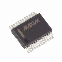
MAX3681EAG+ Maxim Integrated Products, MAX3681EAG+ Datasheet - Page 4

MAX3681EAG+
Manufacturer Part Number
MAX3681EAG+
Description
IC 1:4 DESERIALIZR W/LVDS 24SSOP
Manufacturer
Maxim Integrated Products
Datasheet
1.MAX3681EAG.pdf
(8 pages)
Specifications of MAX3681EAG+
Function
Deserializer
Data Rate
622Mbps
Input Type
LVDS
Output Type
LVDS
Number Of Inputs
1
Number Of Outputs
4
Voltage - Supply
3 V ~ 3.6 V
Operating Temperature
-40°C ~ 85°C
Mounting Type
Surface Mount
Package / Case
24-SSOP
Maximum Operating Temperature
+ 85 C
Minimum Operating Temperature
- 40 C
Mounting Style
SMD/SMT
Operating Supply Voltage
3.3 V
Lead Free Status / RoHS Status
Lead free / RoHS Compliant
The MAX3681 deserializer uses a 4-bit shift register,
4-bit parallel output register, 2-bit counter, PECL input
buffers, and low-voltage differential-signal (LVDS)
input/output buffers to convert 622Mbps serial data to
4-bit-wide, 155Mbps parallel data (Figure 1).
The input shift register continuously clocks incoming
data on the positive transition of the serial clock (SCLK)
input signal. The 2-bit counter generates a parallel out-
put clock (PCLK) by dividing down the serial clock fre-
quency. The PCLK signal is used to clock the parallel
output register. During normal operation, the counter
divides the SCLK frequency by four, causing the output
register to latch every four bits of incoming serial data.
The synchronization inputs (SYNC+, SYNC-) are used
for data realignment and reframing. When the SYNC
signal is pulsed high for at least two SCLK cycles, the
parallel output data is delayed by one SCLK cycle. This
realignment is guaranteed to occur within two PCLK
cycles of the SYNC signal’s positive transition. As a
result, the first incoming bit of data during that PCLK
cycle is dropped, shifting the alignment between PCLK
and data by one bit.
See Figure 2 for the functional timing diagram and
Figure 3 for the timing parameters diagram.
+3.3V, 622Mbps, SDH/SONET
1:4 Deserializer with LVDS Outputs
4
_______________Detailed Description
______________________________________________________________Pin Description
16, 18, 20, 23
17, 19, 21, 24 PD0+ to PD3+
1, 2, 5, 8, 12
9, 15, 22
_______________________________________________________________________________________
PIN
10
11
13
14
3
4
6
7
PD0- to PD3-
SYNC+
SCLK+
PCLK+
SYNC-
NAME
SCLK-
PCLK-
GND
SD+
V
SD-
CC
+3.3V Supply Voltage
Noninverting PECL Serial Data Input. Data is clocked on the SCLK signal’s positive transition.
Inverting PECL Serial Data Input. Data is clocked on the SCLK signal’s positive transition.
Noninverting PECL Serial Clock Input
Inverting PECL Serial Clock Input
Ground
Noninverting LVDS Synchronizing Pulse Input. Pulse the SYNC signal high for at least two SCLK
periods to shift the data alignment by dropping one bit.
Inverting LVDS Synchronizing Pulse Input. Pulse the SYNC signal high for at least two SCLK
periods to shift the data alignment by dropping one bit.
Inverting LVDS Parallel Clock Output
Noninverting LVDS Parallel Clock Output
Inverting LVDS Parallel Data Outputs. Data is updated on the positive transition of the PCLK signal.
See Figure 2 for the relationship between serial-data-bit position and output-data-bit assignment.
Noninverting LVDS Parallel Data Outputs. Data is updated on the positive transition of the PCLK signal.
See Figure 2 for the relationship between serial-data-bit position and output-data-bit assignment.
Figure 1. Functional Diagram
SYNC+
SCLK+
SYNC-
SCLK-
SD+
SD-
FUNCTION
100Ω
PECL
PECL
LVDS
MAX3681
REGISTER
SHIFT
4-BIT
COUNTER
2-BIT
PARALLEL
REGISTER
OUTPUT
4-BIT
LVDS
LVDS
LVDS
LVDS
LVDS
PD3+
PD3-
PD2+
PD2-
PD1+
PD1-
PD0+
PD0-
PCLK+
PCLK-


