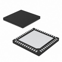
MAX9217ETM+T Maxim Integrated Products, MAX9217ETM+T Datasheet

MAX9217ETM+T
Specifications of MAX9217ETM+T
Related parts for MAX9217ETM+T
MAX9217ETM+T Summary of contents
Page 1
... RGB_IN8 47 RGB_IN9 48 + LQFP ________________________________________________________________ Maxim Integrated Products For pricing, delivery, and ordering information, please contact Maxim Direct at 1-888-629-4642, or visit Maxim’s website at www.maxim-ic.com. 27-Bit, 3MHz-to-35MHz DC-Balanced LVDS Serializer ♦ Proprietary Data Encoding for DC Balance and Reduced EMI ♦ Control Data Sent During Video Blanking ♦ ...
Page 2
DC-Balanced LVDS Serializer ABSOLUTE MAXIMUM RATINGS V to _GND........................................................-0.5V to +4.0V CC_ Any Ground to Any Ground...................................-0.5V to +0.5V OUT+, OUT- to LVDS GND ...................................-0.5V to +4.0V OUT+, OUT- Short Circuit to LVDS GND or V .............................................................Continuous CCLVDS ...
Page 3
DC ELECTRICAL CHARACTERISTICS (continued) = 100Ω ±1%, PWRDWN = high +3.0V to +3.6V, R CC_ +3.3V +25°C.) (Notes 1, 2) CC_ A PARAMETER SYMBOL Differential Output Resistance Worst-Case Supply Current Power-Down Supply ...
Page 4
DC-Balanced LVDS Serializer AC ELECTRICAL CHARACTERISTICS (continued +3.0V to +3.6V 100Ω ±1%, C CC_ L are +3.3V +25°C.) (Note 4) CC_ A PARAMETER SYMBOL Peak-to-Peak Output Offset V Voltage ...
Page 5
PIN NAME 1, 13, 37 GND Input Buffer Supply and Digital Supply Ground Input Buffer Supply Voltage. Bypass to GND with 0.1µF and 0.001µF capacitors in parallel CCIN close to the device as possible, with the smallest ...
Page 6
DC-Balanced LVDS Serializer RGB_IN CNTL_IN DE_IN PCLK_IN RNG0 RNG1 PWRDWN OUT- V (-) OS OUT+ V (-) OD (OUT+) - (OUT-) Figure 1. LVDS DC Output Load and Parameters 6 _______________________________________________________________________________________ 1 DC BALANCE/ INPUT LATCH PAR-TO-SER ENCODE ...
Page 7
PCLK_IN t F Figure 2. Parallel Clock Requirements (OUT+) - (OUT-) Figure 3. Output Rise and Fall Times PCLK_IN RGB_IN[17:0] CNTL_IN[8:0] DE_IN Figure 4. Synchronous Input Timing _______________________________________________________________________________________ 27-Bit, 3MHz-to-35MHz DC-Balanced LVDS Serializer LOW OUT+ OUT- C ...
Page 8
DC-Balanced LVDS Serializer RGB_IN CNTL_IN PCLK_IN OUT_ Figure 5. Serializer Delay PWRDWN HIGH-Z (OUT+) - (OUT-) PCLK_IN Figure 6. PLL Lock Time PWRDWN (OUT+) - (OUT-) PCLK_IN Figure 7. Power-Down Delay 8 _______________________________________________________________________________________ EXPANDED ...
Page 9
OUT- OUT+ ((OUT+) + (OUT-)) / 2 Figure 8. Peak-to-Peak Output Offset Voltage Detailed Description The MAX9217 DC-balanced serializer operates at a parallel clock frequency of 3MHz to 35MHz, serializing 18 bits of parallel video data RGB_IN[17:0] when the data ...
Page 10
DC-Balanced LVDS Serializer TRANSITION CONTROL PHASE PHASE PCLK_IN CNTL_IN DE_IN RGB_IN = NOT SAMPLED BY PCLK_IN Figure 9. Transition Timing Transition Timing The transition words require interconnect bandwidth and displace control data. Therefore, control data is not sampled ...
Page 11
RGB_IN 1 0 CNTL_IN DE_IN PCLK_IN TIMING AND RNG0 PLL CONTROL RNG1 PWRDWN MAX9217 CERAMIC RF SURFACE-MOUNT CAPACITOR *CAPACITORS CAN BE AT EITHER END. Figure 10. AC-Coupled Serializer and Deserializer with Two Capacitors per Link RGB_IN 1 0 CNTL_IN DE_IN ...
Page 12
DC-Balanced LVDS Serializer AC-COUPLING CAPACITOR VALUE vs. PARALLEL CLOCK FREQUENCY 140 125 FOUR CAPACITORS PER LINK 110 TWO CAPACITORS PER LINK PARALLEL CLOCK FREQUENCY (MHz) Figure 12. AC-Coupling ...
Page 13
Power-Down and Power-Off Driving PWRDWN low stops the PLL, switches out the integrated 100Ω output termination, and puts the output in high impedance to ground and differentially. With PWRDWN ≤ 0.3V and all LVTTL/LVCMOS inputs ≤ 0.3V or ≥ V ...
Page 14
DC-Balanced LVDS Serializer Separate the LVTTL/LVCMOS inputs and LVDS output to prevent crosstalk. A four-layer PCB with separate layers for power, ground, and signals is recommended. The MAX9217 ESD tolerance is rated for Human Body Model, Machine Model, ...
Page 15
... Maxim cannot assume responsibility for use of any circuitry other than circuitry entirely embodied in a Maxim product. No circuit patent licenses are implied. Maxim reserves the right to change the circuitry and specifications without notice at any time. Maxim Integrated Products, 120 San Gabriel Drive, Sunnyvale, CA 94086 408-737-7600 ____________________ 15 © 2009 Maxim Integrated Products ...


