MAX9250ECM+T Maxim Integrated Products, MAX9250ECM+T Datasheet - Page 8
MAX9250ECM+T
Manufacturer Part Number
MAX9250ECM+T
Description
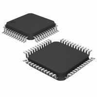
IC DESERIALIZER LVDS 48-LQFP
Manufacturer
Maxim Integrated Products
Datasheet
1.MAX9250ECMT.pdf
(20 pages)
Specifications of MAX9250ECM+T
Function
Deserializer
Data Rate
840Mbps
Input Type
LVDS
Output Type
LVCMOS
Number Of Inputs
1
Number Of Outputs
27
Voltage - Supply
3 V ~ 3.6 V
Operating Temperature
-40°C ~ 85°C
Mounting Type
Surface Mount
Package / Case
48-LQFP
Lead Free Status / RoHS Status
Lead free / RoHS Compliant


27-Bit, 2.5MHz to 42MHz
DC-Balanced LVDS Deserializers
8
MAX9248 MAX9250
REFCLK
29–36,
39–48
IN+
IN-
_______________________________________________________________________________________
27
28
—
PIN
TIMING AND
29–36,
39–48
CONTROL
27
28
14
PLL
RGB_OUT0–
RGB_OUT8–
RGB_OUT17
RBG_OUT7,
PCLK_OUT
OUTEN
NAME
LOCK
RNG[0:1]
SSPLL
1
0
MAX9248
LVTTL/LVCMOS Lock Indicator Output. Outputs are valid when LOCK is low.
LV TTL/LV C M OS P ar al lel Cl ock Outp ut. Latches d ata i nto the next chi p on the ed g e selected b y R/F.
LVTTL/LVCMOS Red, Green, and Blue Digital Video Data Outputs. RGB_OUT[17:0] are
latched into the next chip on the edge of PCLK_OUT selected by R/F when DE_OUT is high,
and are held at the last state when DE_OUT is low.
LVTTL/LVCMOS Output Enable Input. High activates the single-ended outputs. Driving
low places the single-ended outputs in high impedance except LOCK. Internally pulled
down to GND.
PCLK_OUT
R/F
RGB_OUT
CNTL_OUT
DE_OUT
SS
PWRDWN
LOCK
REFCLK
IN+
IN-
FUNCTION
Pin Description (continued)
TIMING AND
CONTROL
PLL
Functional Diagram
RNG[0:1]
MAX9250
1
0
PCLK_OUT
R/F
OUTEN
RGB_OUT
CNTL_OUT
DE_OUT
REF_IN
PWRDWN
LOCK
Related parts for MAX9250ECM+T
Image
Part Number
Description
Manufacturer
Datasheet
Request
R

Part Number:
Description:
MAX7528KCWPMaxim Integrated Products [CMOS Dual 8-Bit Buffered Multiplying DACs]
Manufacturer:
Maxim Integrated Products
Datasheet:
Part Number:
Description:
Single +5V, fully integrated, 1.25Gbps laser diode driver.
Manufacturer:
Maxim Integrated Products
Datasheet:
Part Number:
Description:
Single +5V, fully integrated, 155Mbps laser diode driver.
Manufacturer:
Maxim Integrated Products
Datasheet:
Part Number:
Description:
VRD11/VRD10, K8 Rev F 2/3/4-Phase PWM Controllers with Integrated Dual MOSFET Drivers
Manufacturer:
Maxim Integrated Products
Datasheet:
Part Number:
Description:
Highly Integrated Level 2 SMBus Battery Chargers
Manufacturer:
Maxim Integrated Products
Datasheet:
Part Number:
Description:
Current Monitor and Accumulator with Integrated Sense Resistor; ; Temperature Range: -40°C to +85°C
Manufacturer:
Maxim Integrated Products
Part Number:
Description:
TSSOP 14/A�/RS-485 Transceivers with Integrated 100O/120O Termination Resis
Manufacturer:
Maxim Integrated Products
Part Number:
Description:
TSSOP 14/A�/RS-485 Transceivers with Integrated 100O/120O Termination Resis
Manufacturer:
Maxim Integrated Products
Part Number:
Description:
QFN 16/A�/AC-DC and DC-DC Peak-Current-Mode Converters with Integrated Step
Manufacturer:
Maxim Integrated Products
Part Number:
Description:
TDFN/A/65V, 1A, 600KHZ, SYNCHRONOUS STEP-DOWN REGULATOR WITH INTEGRATED SWI
Manufacturer:
Maxim Integrated Products
Part Number:
Description:
Integrated Temperature Controller f
Manufacturer:
Maxim Integrated Products
Part Number:
Description:
SOT23-6/I�/45MHz to 650MHz, Integrated IF VCOs with Differential Output
Manufacturer:
Maxim Integrated Products
Part Number:
Description:
SOT23-6/I�/45MHz to 650MHz, Integrated IF VCOs with Differential Output
Manufacturer:
Maxim Integrated Products
Part Number:
Description:
EVALUATION KIT/2.4GHZ TO 2.5GHZ 802.11G/B RF TRANSCEIVER WITH INTEGRATED PA
Manufacturer:
Maxim Integrated Products
Part Number:
Description:
QFN/E/DUAL PCIE/SATA HIGH SPEED SWITCH WITH INTEGRATED BIAS RESISTOR
Manufacturer:
Maxim Integrated Products
Datasheet: