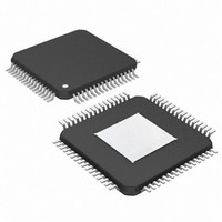
MAX3890ECB+D Maxim Integrated Products, MAX3890ECB+D Datasheet - Page 7

MAX3890ECB+D
Manufacturer Part Number
MAX3890ECB+D
Description
IC 16:1 SERIALIZER 64-TQFP-EP
Manufacturer
Maxim Integrated Products
Datasheet
1.MAX3890ECBD.pdf
(12 pages)
Specifications of MAX3890ECB+D
Function
Serializer
Data Rate
2.5Gbps
Input Type
LVDS
Output Type
PECL
Number Of Inputs
16
Number Of Outputs
1
Voltage - Supply
3 V ~ 3.6 V
Operating Temperature
-40°C ~ 85°C
Mounting Type
Surface Mount
Package / Case
64-TQFP Exposed Pad, 64-eTQFP, 64-HTQFP, 64-VQFP
Lead Free Status / RoHS Status
Lead free / RoHS Compliant
The MAX3890 has LVDS inputs and outputs for inter-
facing with high-speed digital circuitry. The LVDS
standard is based on the IEEE 1596.3 LVDS specifi-
cation. This technology uses 250mV to 400mV differ-
ential low-voltage swings to achieve fast transition
times, minimized power dissipation, and noise immu-
nity.
For proper operation, the parallel clock LVDS outputs
(PCLKO+, PCLKO-) require 100Ω differential DC termi-
nation between the inverting and noninverting outputs.
Do not terminate these outputs to ground.
The parallel data and parallel clock LVDS inputs
(PDI_+, PDI_-, PCLKI+, PCLKI-, RCLK+, RCLK-) are
Figure 2. Timing Diagram
+3.3V, 2.5Gbps, SDH/SONET 16:1 Serializer
OUTPUT DATA
INPUT DATA
PARALLEL
Low-Voltage Differential-Signal
SERIAL
PCLKO
(PDI_)
PCLKI
(SDO)
_______________________________________________________________________________________
NOTE: SIGNALS SHOWN ARE DIFFERENTIAL. FOR EXAMPLE, PCLKO = (PCLKO+) - (PCLKO-).
*PDI 15 = D15; PDI14 = D14; ...PDI0 = D0.
THIS FIGURE IS NOT INTENDED TO SHOW A SPECIFIC TIMING RELATIONSHIP BETWEEN PARALLEL
INPUT DATA AND SERIAL OUTPUT DATA.
with Clock Synthesis and LVDS Inputs
Inputs and Outputs
VALID PARALLEL DATA*
t
SU
t
SKEW
t
H
internally terminated with 100Ω differential input resis-
tance, and therefore do not require external termina-
tion.
The serial-data PECL outputs (SDO+, SDO-, SCLKO+,
SCLKO-) require 50Ω DC termination to (V
the Alternative PECL-Output Termination section).
The system loopback outputs (SLBO+, SLBO-) of the
MAX3890 are designed using CML. The configuration
of the MAX3890 current-mode logic (CML) output cir-
cuit includes internal 50Ω back termination to V
(Figure 3). These outputs are intended to drive a 50Ω
transmission line terminated with a matched load
impedance.
Current-Mode Logic Outputs
PECL Outputs
CC
- 2V) (see
CC
7


