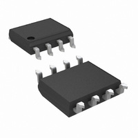
DS92001TMA/NOPB National Semiconductor, DS92001TMA/NOPB Datasheet - Page 2

DS92001TMA/NOPB
Manufacturer Part Number
DS92001TMA/NOPB
Description
IC BLVDS-BLVDS BUFFER 3.3V 8SOIC
Manufacturer
National Semiconductor
Type
Bufferr
Datasheet
1.DS92001TMANOPB.pdf
(12 pages)
Specifications of DS92001TMA/NOPB
Tx/rx Type
LVDS
Delay Time
2.0ns
Voltage - Supply
3 V ~ 3.6 V
Current - Supply
65mA
Mounting Type
Surface Mount
Package / Case
8-SOIC (3.9mm Width)
Supply Current
20µA
Supply Voltage Range
3V To 3.6V
Driver Case Style
SOIC
No. Of Pins
8
Operating Temperature Range
-40°C To +85°C
Msl
MSL 1 - Unlimited
Voltage, Vcc
4V
Filter Terminals
SMD
Rohs Compliant
Yes
Data Rate
400Mbps
Data Rate Max
400Mbps
Lead Free Status / RoHS Status
Lead free / RoHS Compliant
Capacitance - Input
-
Other names
*DS92001TMA
*DS92001TMA/NOPB
DS92001TMA
*DS92001TMA/NOPB
DS92001TMA
Available stocks
Company
Part Number
Manufacturer
Quantity
Price
Company:
Part Number:
DS92001TMA/NOPB
Manufacturer:
Intel
Quantity:
20
Part Number:
DS92001TMA/NOPB
Manufacturer:
TI/德州仪器
Quantity:
20 000
www.national.com
LVCMOS/LVTTL DC SPECIFICATIONS (EN)
V
V
I
I
V
BLVDS OUTPUT DC SPECIFICATIONS (OUT)
|V
ΔV
V
ΔV
I
I
I
I
Symbol
IH
IL
OZ
OFF
OS1
OSD
Supply Voltage (V
LVCMOS/LVTTL Input Voltage
(EN)
B/LVDS Receiver Input Voltage
(IN+, IN−)
BLVDS Driver Output Voltage
(OUT+, OUT−)
BLVDS Output Short Circuit
Current
Junction Temperature
Storage Temperature Range
Lead Temperature Range
IH
IL
CL
OS
OD
Absolute Maximum Ratings
If Military/Aerospace specified devices are required,
please contact the National Semiconductor Sales Office/
Distributors for availability and specifications.
Electrical Characteristics
Over recommended operating supply and temperature ranges unless otherwise specified. (Notes 2, 3)
OD
OS
Soldering (4 sec.)
|
High Level Input Voltage
Low Level Input Voltage
High Level Input Current
Low Level Input Current
Input Clamp Voltage
Differential Output Voltage (Note
2)
Change in Magnitude of V
Complimentary Output States
Offset Voltage
Change in Magnitude of V
Complimentary Output States
Output TRI-STATE Current
Power-Off Leakage Current
Output Short Circuit Current (Note
4)
Differential Output Short Circuit
Current (Note 4)
CC
)
Parameter
OD
OS
for
for
−0.3V to (V
V
V
I
R
R
RL = 27Ω or 50Ω Figure 1, Figure 2
R
Figure 1
EN = 0V, V
V
EN = V
V
V
V
EN = V
(connect true and complement outputs through a
current meter)
−65°C to +150°C
CL
IN
IN
L
L
L
CC
ID
ID
ID
= 27Ω
= 50Ω
= 27Ω or R
= −18 mA
= V
= GND or 0.8V
= −200mV, V
= −200mV, V
= 200mV, V
(Note 1)
−0.3V to +4V
−0.3V to +4V
−0.3V to +4V
= 0V or Open Circuit, V
Continuous
CC
CC
CC
CC
, V
, V
+150°C
+260°C
+ 0.3V)
or 2.0V
OUT
CM
ID
L
= |200mV|, V
= V
= 1.2V,V
CM
= 50Ω
CM
CM
CC
=1.2V, V
2
= 1.2V, V
= 1.2V, V
Conditions
or GND
Maximum Package Power Dissipation at 25°C
ESD Ratings
ID
Recommended Operating
Conditions
Supply Voltage (V
Receiver Differential Input
Voltage (V
V
Operating Free Air
Temperature
B/LVDS Input Rise/Fall
20% to 80%
M Package
Derate M Package
LDA Package
Derate LDA Package
(HBM, 1.5kΩ, 100pF)
(EIAJ, 0Ω, 200pF)
= 200mV, V
CM
OUT−
CM
OUT
=1.2V
OUT−
OUT+
. = 1.2V, V
= 3.6V
= V
= 0V
= V
ID
CC
) with
CC
OUT+
OD
, or
CC
= 0V, or
= 0V
)
Min
−40
3.0
0.1
GND
Min
−10
250
350
−20
−20
2.0
1.1
19.49 mW/°C above +25°C
5.8 mW/°C above +25°C
Typ
+25
3.3
2
−0.6
1.25
Typ
350
450
−30
|30|
+7
±1
±5
±5
53
2
Max
+85
3.6
2.4
20
1.375
Max
−1.5
V
+20
+10
500
600
+20
+20
−60
|42|
0.8
20
20
80
CC
726 mW
Units
≥
2.44 W
≥
|V|
°C
ns
V
2.5kV
250V
Units
mV
mV
mV
mV
mA
mA
mA
μA
μA
μA
μA
V
V
V
V


