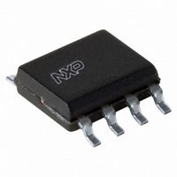
P82B96TD,112 NXP Semiconductors, P82B96TD,112 Datasheet - Page 17

P82B96TD,112
Manufacturer Part Number
P82B96TD,112
Description
IC I2C BUS BUFFER DUAL 8-SOIC
Manufacturer
NXP Semiconductors
Type
Bufferr
Datasheet
1.P82B96TD118.pdf
(32 pages)
Specifications of P82B96TD,112
Package / Case
8-SOIC (3.9mm Width)
Tx/rx Type
I²C Logic
Delay Time
5.0ns
Capacitance - Input
7pF
Voltage - Supply
2 V ~ 15 V
Current - Supply
900µA
Mounting Type
Surface Mount
Logic Family
P82B
Supply Voltage (max)
15 V
Supply Voltage (min)
2 V
Maximum Operating Temperature
85 C
Mounting Style
SMD/SMT
Maximum Power Dissipation
300 mW
Minimum Operating Temperature
- 40 C
Number Of Lines (input / Output)
4 / 2
Propagation Delay Time
90 ns
Logic Type
Bus Buffer
Lead Free Status / RoHS Status
Lead free / RoHS Compliant
For Use With
OM6285 - EVAL BOARD I2C-2002-1A568-4002 - DEMO BOARD I2C
Lead Free Status / Rohs Status
Lead free / RoHS Compliant
Other names
568-3982-5
935262295112
P82B96TD
P82B96TD
935262295112
P82B96TD
P82B96TD
NXP Semiconductors
P82B96_8
Product data sheet
Fig 18. I
SDA
SCL
2
C-bus multipoint application
3.3 V to 5 V
3.3 V to 5 V
edge from the master reaching the slave
the SCL rising edge
SDA, reaching the master
The master microcontroller should be programmed to produce a nominal SCL LOW
period = (1300 + A
minimum SCL HIGH period of 600 ns. Then a check should be made to ensure the cycle
time is not shorter than the minimum 2500 ns. If found necessary, just increase either
clock period.
Due to clock stretching, the SCL cycle time will always be longer than
(600 + 1300 + A + C) ns.
Example:
Sx
Sy
The master bus has an RmCm product of 100 ns and V
The buffered bus has a capacitance of 1 nF and a pull-up resistor of 160
an RbCb product of 160 ns. The slave bus also has an RsCs product of 100 ns.
The microcontroller LOW period should be programmed to
Its HIGH period may be programmed to the minimum 600 ns.
The nominal microcontroller clock period will be
equivalent to a frequency of 442 kHz.
The actual bus clock period, including the 482 ns clock stretch effect, will be below
(nominal + stretch) = (2262.5 + 482) ns or
frequency of 364 kHz.
P82B96
(1300 + 372.5
12 V
Tx
Rx
Ty
Ry
12 V
12 V
no limit to the number of connected bus devices
482 + 472) ns, that is
(Figure
Rev. 08 — 10 November 2009
B + C) ns, and should be programmed to produce the nominal
Sx
SCL/SDA
P82B96
(Figure
16) plus total delays in the slave's response data, carried on
Sy
Sx
17).
P82B96
SCL/SDA
Sy
(Figure
Sx
SCL/SDA
P82B96
1662.5 ns.
2745 ns, equivalent to an allowable
Sy
15) minus the effective delay (stretch) of
(1662.5 + 600) ns = 2262.5 ns,
P82B96
CCM
Dual bidirectional bus buffer
3.3 V 3.3 V
twitsted-pair telephone wires,
USB, or flat ribbon cables;
up to 15 V logic levels,
include V
= 5 V.
CC
and GND
Sy SDA
Sx SCL
© NXP B.V. 2009. All rights reserved.
P82B96
002aab994
to 5 V giving
17 of 32


