MAX7359ETG+ Maxim Integrated Products, MAX7359ETG+ Datasheet
MAX7359ETG+
Specifications of MAX7359ETG+


Related parts for MAX7359ETG+


MAX7359ETG+ Summary of contents
Page 1
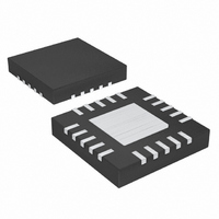
... Up to Seven Open-Drain Logic Outputs Available Capable of Driving LEDs o 400kbps, 5.5V-Tolerant, 2-Wire Serial Interface o Selectable 2-Wire, Serial-Bus Timeout o Four Address Choices o Small, 24-Pin TQFN Package (3.5mm x 3.5mm 25-Pin WLP Package (2.31mm x 2.31mm) PART MAX7359ETG+ Applications MAX7359EWA+ + Denotes a lead(Pb)-free/RoHS-compliant package Exposed pad. TOP VIEW 8 SWITCH ARRAY ...
Page 2
Interfaced Low-EMI Key Switch Controller/GPO ABSOLUTE MAXIMUM RATINGS (All voltages referenced to GND.) V ..........................................................................-0.3V to +4V CC COL2/PORT2–COL7/PORT7 ....................................-0.3V to +4V SDA, SCL, AD0, INT .................................................-0.3V to +6V All Other Pins ..............................................-0. Current on COL2/PORT2–COL7/PORT7 ...
Page 3
I C TIMING CHARACTERISTICS (V = +1.62V to +3.6V MIN PARAMETER SYMBOL Input Capacitance (SCL, SDA, AD0) SCL Serial-Clock Frequency Bus Free Time Between a STOP and a START Condition Hold Time ...
Page 4
Interfaced Low-EMI Key Switch Controller/GPO (V = +2.5V +25°C, unless otherwise noted GPO PORT OUTPUT LOW VOLTAGE vs. SINK CURRENT 300 V = +2.4V CC 250 T = +85°C A 200 150 100 T = ...
Page 5
MAX7359 64kHz OSCILLATOR INT CONTROL SDA REGISTERS SCL FIFO INTERFACE BUS POR TIMEOUT *GPO _______________________________________________________________________________________ 2-Wire Interfaced Low-EMI Key Switch Controller/GPO Functional Block Diagram COLUMN ENABLE CURRENT GPO ENABLE SOURCE COLUMN CURRENT DETECT DRIVES KEY SCAN OPEN- ...
Page 6
Interfaced Low-EMI Key Switch Controller/GPO PIN NAME TQFN WLP 1 A1 ROW2 Row Input from Key Matrix. Leave ROW2 unconnected or connect to GND if unused ROW3 Row Input from Key Matrix. Leave ROW3 unconnected or connect ...
Page 7
Key-Scan Controller Key inputs are scanned statically, not dynamically, to ensure low-EMI operation. As inputs only toggle in response to switch changes, the key matrix can be routed closer to sensitive circuit nodes. The key controller debounces and maintains a ...
Page 8
Interfaced Low-EMI Key Switch Controller/GPO Table 3. Keys FIFO Register Format (0x00) SPECIAL FUNCTION The key number indicated by D5: key event always for a key press of key 62 and key 63. When D7 ...
Page 9
Table 4. Configuration Register Format (0x01) REGISTER BIT DESCRIPTION D7 Sleep D6 Reserved D5 INTERRUPT D4 Reserved D3 Key release enable D2 Reserved D1 Wakeup D0 Timeout enable _______________________________________________________________________________________ 2-Wire Interfaced Low-EMI Key Switch Controller/GPO VALUE FUNCTION ...
Page 10
Interfaced Low-EMI Key Switch Controller/GPO Debounce Register (0x02) The debounce register sets the time for each debounce cycle, as well as setting whether the GPO ports are enabled or disabled. Bits D0 through D4 set the debounce time in ...
Page 11
Interrupt Register (0x03) The interrupt register contains information related to the settings of the interrupt request function, as well as the status of the INT output, which can also be configured as a GPO. If bits D0 through D7 are ...
Page 12
Interfaced Low-EMI Key Switch Controller/GPO Table 7. Ports Register Format (0x04) REGISTER BIT DESCRIPTION D7 PORT 7 Control D6 PORT 6 Control D5 PORT 5 Control D4 PORT 4 Control D3 PORT 3 Control D2 PORT 2 Control INT ...
Page 13
Only one autorepeat code is entered into the FIFO, regard- less of the number of keys pressed. The autorepeat code continues to be entered in the FIFO at the frequency set by the bits D4–D1 until another key event is ...
Page 14
Interfaced Low-EMI Key Switch Controller/GPO SDA t SU, DAT t LOW t SCL HIGH t HD, STA t R START CONDITION Figure 1. 2-Wire Serial Interface Timing Details SDA SCL S START CONDITION Figure 2. START and STOP Conditions ...
Page 15
The acknowledge bit is a clocked 9th bit (Figure 4), which the recipient uses to handshake receipt of each byte of data. Thus, each byte transferred effectively requires 9 bits. The master generates the 9th clock pulse, and the recipient ...
Page 16
Interfaced Low-EMI Key Switch Controller/GPO COMMAND BYTE IS STORED ON RECEIPT OF ACKNOWLEDGE CONDITION ACKNOWLEDGE FROM MAX7359 S SLAVE ADDRESS Figure 6. Command Byte Received ACKNOWLEDGE FROM MAX7359 S SLAVE ADDRESS 0 R/W Figure 7. Command and Single Data ...
Page 17
ACKNOWLEDGE FROM MAX7359 S SLAVE ADDRESS R/W Figure 8. N Data Bytes Received Command Address Autoincrementing Address autoincrementing allows the MAX7359 to be configured with fewer transmissions by minimizing the number of times the command address needs to be sent. ...
Page 18
Interfaced Low-EMI Key Switch Controller/GPO REGULAR KEY-PRESS EVENT KEY-SWITCH MATRIX Figure 9. Ghost-Key Phenomenon +3.3V +3.3V +1. COL6/PORT6 COL7/PORT7 AD0 MAX7359 + SCL SCL µC SDA SDA INT INT GND GND 18 ______________________________________________________________________________________ GHOST-KEY EVENT ...
Page 19
Pin Configurations (continued) TOP VIEW (BUMPS ON BOTTOM) MAX7359 COL3/ ROW2 ROW3 ROW4 PORT3 A COL4/ ROW1 ROW0 ROW7 PORT4 B COL7/ COL5/ N.C. N.C. PORT7 PORT5 C V SCL GND CC D INT SDA AD0 ...
Page 20
... Maxim cannot assume responsibility for use of any circuitry other than circuitry entirely embodied in a Maxim product. No circuit patent licenses are implied. Maxim reserves the right to change the circuitry and specifications without notice at any time. 20 ____________________Maxim Integrated Products, 120 San Gabriel Drive, Sunnyvale, CA 94086 408-737-7600 © 2010 Maxim Integrated Products ...