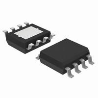
AOZ1034DI Alpha & Omega Semiconductor Inc, AOZ1034DI Datasheet - Page 10

AOZ1034DI
Manufacturer Part Number
AOZ1034DI
Description
IC BUCK SYNC ADJ 4A 8DFN
Manufacturer
Alpha & Omega Semiconductor Inc
Series
EZBuck™r
Type
Step-Down (Buck), PWM - Current Moder
Datasheet
1.AOZ1034DI.pdf
(18 pages)
Specifications of AOZ1034DI
Featured Product
The AOZ103x Family Synchronous Buck Regulator
Internal Switch(s)
Yes
Synchronous Rectifier
Yes
Number Of Outputs
1
Voltage - Output
0.8 V ~ 18 V
Current - Output
4A
Frequency - Switching
500kHz
Voltage - Input
4.5 V ~ 18 V
Operating Temperature
-40°C ~ 85°C
Mounting Type
Surface Mount
Package / Case
8-VDFN Exposed Pad
Lead Free Status / Rohs Status
Lead free / RoHS Compliant
Other names
785-1254-2
Available stocks
Company
Part Number
Manufacturer
Quantity
Price
Output ripple voltage specification is another important
factor for selecting the output capacitor. In a buck
converter circuit, output ripple voltage is determined by
inductor value, switching frequency, output capacitor
value and ESR. It can be calculated by the equation
below:
where;
C
ESR
When low ESR ceramic capacitor is used as output
capacitor, the impedance of the capacitor at the switching
frequency dominates. Output ripple is mainly caused by
capacitor value and inductor ripple current. The output
ripple voltage calculation can be simplified to:
If the impedance of ESR at switching frequency
dominates, the output ripple voltage is mainly decided by
capacitor ESR and inductor ripple current. The output
ripple voltage calculation can be further simplified to:
For lower output ripple voltage across the entire
operating temperature range, X5R or X7R dielectric type
of ceramic, or other low ESR tantalum are recommended
to be used as output capacitors.
In a buck converter, output capacitor current is
continuous. The RMS current of output capacitor is
decided by the peak to peak inductor ripple current.
It can be calculated by:
Usually, the ripple current rating of the output capacitor
is a smaller issue because of the low current stress.
When the buck inductor is selected to be very small and
inductor ripple current is high, output capacitor could be
overstressed.
External Schottky Diode for High Input Operation
When V
diode is required between LX and PGND for proper
operation.
I
ΔV
ΔV
ΔV
CO_RMS
O
Rev. 1.1 September 2010
is output capacitor value, and
CO
O
O
O
=
is the Equivalent Series Resistor of output capacitor.
=
=
IN
ΔI
ΔI
ΔI
is higher than 16V, an external 1A schottky
=
L
L
L
×
----------
×
×
ΔI
12
ESR
⎛
⎝
-------------------------
8
L
ESR
×
f C
1
×
CO
CO
O
+
-------------------------
8
×
f C
1
×
O
⎞
⎠
www.aosmd.com
Loop Compensation
The AOZ1034 employs peak current mode control for
easy use and fast transient response. Peak current mode
control eliminates the double pole effect of the output
L&C filter. It greatly simplifies the compensation loop
design.
With peak current mode control, the buck power stage
can be simplified to be a one-pole and one-zero system
in frequency domain. The pole is dominant pole can be
calculated by:
The zero is a ESR zero due to output capacitor and its
ESR. It is can be calculated by:
where;
C
R
ESR
The compensation design is actually to shape the
converter control loop transfer function to get desired
gain and phase. Several different types of compensation
network can be used for the AOZ1034. For most cases, a
series capacitor and resistor network connected to the
COMP pin sets the pole-zero and is adequate for a stable
high-bandwidth control loop.
In the AOZ1034, FB pin and COMP pin are the inverting
input and the output of internal error amplifier. A series
R and C compensation network connected to COMP
provides one pole and one zero. The pole is:
where;
G
200 x 10
G
C
The zero given by the external compensation network,
capacitor C
f
f
f
P2
O
L
EA
VEA
C
Z2
Z1
f
P1
is load resistor value, and
is compensation capacitor in Figure 1.
is the output filter capacitor,
CO
is the error amplifier transconductance, which is
=
=
=
is the error amplifier voltage gain, which is 500 V/V, and
=
is the equivalent series resistance of output capacitor.
-6
------------------------------------------ -
2π
-----------------------------------
2π
------------------------------------------------
2π
---------------------------------- -
2π
A/V,
×
C
×
×
×
and resistor R
C
C
C
G
1
C
C
C
O
1
EA
O
×
×
1
×
×
R
G
ESR
R
C
VEA
L
CO
C
, is located at:
AOZ1034
Page 10 of 18


