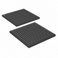
DS33W41+ Maxim Integrated Products, DS33W41+ Datasheet - Page 368

DS33W41+
Manufacturer Part Number
DS33W41+
Description
IC MAPPING ETHERNET 256CSBGA
Manufacturer
Maxim Integrated Products
Datasheet
1.DS33X11.pdf
(375 pages)
Specifications of DS33W41+
Applications
Data Transport
Interface
Parallel/Serial
Voltage - Supply
1.8V, 2.5V, 3.3V
Package / Case
256-CSBGA
Mounting Type
Surface Mount
Lead Free Status / RoHS Status
Lead free / RoHS Compliant
- Current page: 368 of 375
- Download datasheet (3Mb)
ID code will always have a 1 in the LSB position. The next 11 bits identify the manufacturer’s JEDEC number and
number of continuation bytes followed by 16 bits for the device and 4 bits for the version.
13.3 JTAG ID Codes
Table 13-2. ID Code Structure
13.4 Test Registers
IEEE 1149.1 requires a minimum of two test registers: the bypass register and the boundary scan register. An
optional test register has been included in the device. This test register is the identification register and is used in
conjunction with the IDCODE instruction and the Test-Logic-Reset state of the TAP controller.
13.4.1 Boundary Scan Register
This register contains both a shift register path and a latched parallel output for all control cells and digital I/O cells
and is n bits in length.
13.4.2 Bypass Register
This is a single one-bit shift register used in conjunction with the BYPASS, CLAMP, and HIGHZ instructions, which
provides a short path between JTDI and JTDO.
13.4.3 Identification Register
The identification register contains a 32-bit shift register and a 32-bit latched parallel output. This register is
selected during the IDCODE instruction and when the TAP controller is in the Test-Logic-Reset state.
Rev: 063008
DS33Xyy rev A1
DS33Xyy rev B1
________________________________________________ DS33X162/X161/X82/X81/X42/X41/X11/W41/W11
DEVICE
REVISION
ID[31:28]
0000
0001
0000 0000 0000 0110
0000 0000 0000 0110
DEVICE CODE
ID[27:12]
MANUFACTURER’S CODE
000 1010 0001
000 1010 0001
ID[11:1]
REQUIRED
ID[0]
368 of 375
1
1
Related parts for DS33W41+
Image
Part Number
Description
Manufacturer
Datasheet
Request
R

Part Number:
Description:
MAX7528KCWPMaxim Integrated Products [CMOS Dual 8-Bit Buffered Multiplying DACs]
Manufacturer:
Maxim Integrated Products
Datasheet:

Part Number:
Description:
Single +5V, fully integrated, 1.25Gbps laser diode driver.
Manufacturer:
Maxim Integrated Products
Datasheet:

Part Number:
Description:
Single +5V, fully integrated, 155Mbps laser diode driver.
Manufacturer:
Maxim Integrated Products
Datasheet:

Part Number:
Description:
VRD11/VRD10, K8 Rev F 2/3/4-Phase PWM Controllers with Integrated Dual MOSFET Drivers
Manufacturer:
Maxim Integrated Products
Datasheet:

Part Number:
Description:
Highly Integrated Level 2 SMBus Battery Chargers
Manufacturer:
Maxim Integrated Products
Datasheet:

Part Number:
Description:
Current Monitor and Accumulator with Integrated Sense Resistor; ; Temperature Range: -40°C to +85°C
Manufacturer:
Maxim Integrated Products

Part Number:
Description:
TSSOP 14/A�/RS-485 Transceivers with Integrated 100O/120O Termination Resis
Manufacturer:
Maxim Integrated Products

Part Number:
Description:
TSSOP 14/A�/RS-485 Transceivers with Integrated 100O/120O Termination Resis
Manufacturer:
Maxim Integrated Products

Part Number:
Description:
QFN 16/A�/AC-DC and DC-DC Peak-Current-Mode Converters with Integrated Step
Manufacturer:
Maxim Integrated Products

Part Number:
Description:
TDFN/A/65V, 1A, 600KHZ, SYNCHRONOUS STEP-DOWN REGULATOR WITH INTEGRATED SWI
Manufacturer:
Maxim Integrated Products

Part Number:
Description:
Integrated Temperature Controller f
Manufacturer:
Maxim Integrated Products

Part Number:
Description:
SOT23-6/I�/45MHz to 650MHz, Integrated IF VCOs with Differential Output
Manufacturer:
Maxim Integrated Products

Part Number:
Description:
SOT23-6/I�/45MHz to 650MHz, Integrated IF VCOs with Differential Output
Manufacturer:
Maxim Integrated Products

Part Number:
Description:
EVALUATION KIT/2.4GHZ TO 2.5GHZ 802.11G/B RF TRANSCEIVER WITH INTEGRATED PA
Manufacturer:
Maxim Integrated Products

Part Number:
Description:
QFN/E/DUAL PCIE/SATA HIGH SPEED SWITCH WITH INTEGRATED BIAS RESISTOR
Manufacturer:
Maxim Integrated Products
Datasheet:


