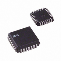
AD7569KP Analog Devices Inc, AD7569KP Datasheet - Page 3

AD7569KP
Manufacturer Part Number
AD7569KP
Description
IC I/O PORT 8BIT ANLG 28-PLCC
Manufacturer
Analog Devices Inc
Series
LC²MOSr
Datasheet
1.AD7569JRZ.pdf
(20 pages)
Specifications of AD7569KP
Rohs Status
RoHS non-compliant
Applications
Analog I/O
Interface
Bus
Voltage - Supply
4.75 V ~ 5.25 V
Package / Case
28-LCC (J-Lead)
Mounting Type
Surface Mount
Converter Type
ADC/DAC
Resolution
8b
Number Of Dac's
Single
Data Rate
0.5MSPS
Digital Interface Type
Parallel
Pin Count
28
Package Type
PLCC
Lead Free Status / Rohs Status
Not Compliant
ADC SPECIFICATIONS
Parameter
DC ACCURACY
DYNAMIC PERFORMANCE
ANALOG INPUT
LOGIC INPUTS
LOGIC OUTPUTS
CONVERSION TIME
POWER REQUIREMENTS
NOTES
1
2
3
4
5
6
7
8
Specifications subject to change without notice.
REV. B
wise noted. All specifications T
Temperature ranges are as follows: J, K versions; 0 C to +70 C
1 LSB = 4.88 mV for 0 V to +1.25 V range, 9.76 mV for 0 V to +2.5 V and 1.25 V ranges and 19.5 mV for +2.5 V range.
See Terminology.
Includes internal voltage reference error and is calculated after offset error has been adjusted out. Ideal unipolar last code transition occurs at (FS – 3/2 LSB). Ideal bipolar last code transition occurs at
Exact frequencies are 101 kHz and 384 kHz to avoid harmonics coinciding with sampling frequency.
Rising edge of BUSY to falling edge of ST. The time given refers to the acquisition time, which gives a 3 dB degradation in SNR from the tested figure.
Sample tested at +25 C to ensure compliance.
Except where noted, specifications apply for all ranges including bipolar ranges with dual supply operation.
(FS/2 – 3/2 LSB).
Resolution
Total Unadjusted Error
Relative Accuracy
Differential Nonlinearity
Unipolar Offset Error
Bipolar Zero Offset Error
Full-Scale Error
Signal-to-Noise Ratio
Total Harmonic Distortion
Intermodulation Distortion
Frequency Response
Track/Hold Acquisition Time
Input Voltage Ranges
Input Current
Input Capacitance
CS, RD, ST, CLK, RESET, RANGE
CS, RD, ST, RANGE, RESET
CLK
DB0–DB7, INT, BUSY
DB0–DB7
Output Coding (Single Supply)
Output Coding (Dual Supply)
With External Clock
With Internal Clock, T
Full Scale/ V
Full Scale/ V
@ +25 C
T
@ +25 C
T
@ +25 C
T
Unipolar
Bipolar
Input Low Voltage, V
Input High Voltage, V
Input Capacitance
Input Leakage Current
Input Current
V
V
Floating State Leakage Current
Floating State Output Capacitance
OL
OH
MIN
MIN
MIN
I
I
INL
INH
, Output Low Voltage
, Output High Voltage
to T
to T
to T
3
MAX
MAX
MAX
DD
SS
5
, T
, T
4
A
A
8
= +25 C
4
= +25 C
(SNR)
A
4
INL
INH
4
= +25 C
4
4
(THD)
(IMD)
7
A, B versions; –40 C to +85 C
S, T versions; –55 C to +125 C
8
MIN
to T
(V
MAX
DD
AD7569
J, A Versions
AD7669
J Version
8
–4, +0
–5.5, +1.5
0.5
0.5
44
48
60
0.1
200
10
0.8
2.4
10
10
–1.6
40
0.4
4.0
10
10
2
1.6
2.6
3
1
1
2
3
3
3.5
300
unless otherwise noted.) Specifications apply to Mode 1 interface.
= +5 V
0 to +1.25/ +2.5
As per DAC Specifications
1.25/ 2.5
3
5%; V
AD7569
K, B
Versions
8
–4, +0
–5.5, +1.5
0.5
0.5
46
48
60
0.1
200
10
0.8
2.4
10
10
–1.6
40
0.4
4.0
10
10
Binary
2
1.6
2.6
3
1/2
3/4
1.5
2.5
2.5
3
300
2s Complement
SS
1
= RANGE = AGND
AD7569
S Version
8
–4, +0
–7.5, +2
0.5
0.5
44
48
60
0.1
300
10
0.8
2.4
10
10
–1.6
40
0.4
4.0
10
10
2
1.6
2.6
4
1
1
2
3
3
4
300
–3–
AD7569
T Version
8
–4, +0
–7.5, +2
0.5
0.5
45
48
60
0.1
300
10
0.8
2.4
10
10
–1.6
40
0.4
4.0
10
10
2
1.6
2.6
4
1/2
3/4
1.5
2.5
2.5
3.5
300
DAC
= AGND
Units
Bits
LSB typ
LSB max
LSB max
LSB max
LSB max
LSB max
LSB max
LSB max
LSB max
LSB max
LSB max
dB min
dB max
dB typ
dB typ
ns typ
Volts
Volts
pF typ
V max
V min
pF max
mA max
V max
V min
pF max
A max
A max
A max
A max
s max
s min
s max
DAC
= DGND = 0 V; f
Conditions/Comments
No Missing Codes
Typical tempco is 10 V/ C for +1.25 V range; V
Typical tempco is 20 V/ C for + 1.25 V range; V
V
V
V
V
V
fa = 99 kHz, fb = 96.7 kHz with f
V
V
V
See equivalent circuit Figure 5
V
V
V
I
I
f
Using recommended clock components shown in Figure 21.
Clock frequency can be adjusted by varying R
CLK
SINK
SOURCE
DD
IN
IN
IN
IN
IN
DD
DD
IN
IN
IN
= +2.5 V; V
= –2.5 V; V
= 100 kHz full-scale sine wave with f
= 100 kHz full-scale sine wave with f
= 2.5 V, dc to 200 kHz sine wave
= 0 V
= V
= 0 to V
= +5 V; V
= 5 V
= +5 V; V
= 5 MHz
= 1.6 mA
DD
= 200 A
DD
SS
SS
CLK
SS
= –5 V
= 0 V
DD
= 5%
= 5 MHz external unless other-
= 5%
AD7569/AD7669
SAMPLING
SAMPLING
SAMPLING
= 400 kHz
CLK
SS
.
SS
= 400 kHz
= 400 kHz
= 0 V
= –5 V
6
6


