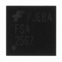
FSA2567MPX Fairchild Semiconductor, FSA2567MPX Datasheet

FSA2567MPX
Specifications of FSA2567MPX
Available stocks
Related parts for FSA2567MPX
FSA2567MPX Summary of contents
Page 1
... Applications Cell phone, PDA, Digital Camera, and Notebook LCD Monitor, TV, and Set-Top Box Ordering Information Operating Part Number Top Mark Temperature FSA2567MPX FSA2567 -40 to +85°C FSA2567UMX GX -40 to +85°C For Fairchild’s definition of Eco Status, please visit: http://www.fairchildsemi.com/company/green/rohs_green.html. © 2008 Fairchild Semiconductor Corporation FSA2567 Rev ...
Page 2
... Through View) Pin Definitions Pin nDAT, nRST, nCLK nV SIM V , DAT, RST, CLK SIM Sel Truth Table Sel Logic LOW Logic HIGH © 2008 Fairchild Semiconductor Corporation FSA2567 Rev. 1.0 DAT 12 11 2DAT No Connect 10 2RST 1CLK 9 8 Multiplexed Data Source Inputs ...
Page 3
... DC Output Current - V SIM I DC Output Current – DAT, CLK, RST OUT T Operating Temperature A Note: 2. The control input must be held HIGH or LOW; it must not float. © 2008 Fairchild Semiconductor Corporation FSA2567 Rev. 1.0.3 Parameter (1) (1) SIM All Pins I/O to GND Parameter (2) SIM 3 Min ...
Page 4
... Measured by the voltage drop between nDAT, nRST, nCLK and relative common port pins at the indicated current through the switch. On resistance is determined by the lower of the voltage on the relative ports. 4. Guaranteed by characterization. © 2008 Fairchild Semiconductor Corporation FSA2567 Rev. 1.0.3 unless otherwise specified. CC ...
Page 5
... BBMV (V ) SIM Charge Injection Q (DAT,CLK,RST) Off Isolation O IRR (DAT,CLK,RST) Non-Adjacent Channel Xtalk Crosstalk (DAT,CLK,RST) -3db Bandwidth BW (DAT,CLK,RST) Note: 5. Guaranteed by characterization. © 2008 Fairchild Semiconductor Corporation FSA2567 Rev. 1.0.3 Conditions R = 50Ω 35pF 1.5V SW Figure 11, Figure 50Ω 35pF 1.5V SW Figure 11, Figure 50Ω, C ...
Page 6
... C RST, CLK, DAT On Capacitance OND Capacitance ONV SIM C RST, CLK, DAT Off Capacitance OFFD C V Off Capacitance OFFV SIM Note: 6. Guaranteed by characterization. © 2008 Fairchild Semiconductor Corporation FSA2567 Rev. 1.0.3 Conditions 3.3V 1MHz (6) CC Figure 3.3V 1MHz (6) CC Figure 3.3V CC Figure ...
Page 7
... Fairchild Semiconductor Corporation FSA2567 Rev. 1.0.3 0.50 0.40 0.30 0.20 0.10 0.00 2.00 3.00 = 2.7V CC Data Path Frequency Response 0 1 Frequency (MHz 2.7V CC Figure 6. Off Isolation Frequency Response 0 1 Frequency (MHz ...
Page 8
... C includes test fixture and stray capacitance. L Figure 11. AC Test Circuit Load nV , nRST , SIM nCLK, or nDAT V SW GND Sel © 2008 Fairchild Semiconductor Corporation FSA2567 Rev. 1.0 RST, SIM CLK, or DAT I ON GND Sel V , RST, SIM ...
Page 9
... S environment (see tables for specific values). Figure 18 nRST , SIM nCLK, or nDAT Capacitance Meter f = 1MHz nV , nRST, SIM nCLK, or nDAT Figure 19. Channel Off Capacitance © 2008 Fairchild Semiconductor Corporation FSA2567 Rev. 1.0.3 V ,RST, SIM CLK or DAT V OUT SW2 GND GND Sel are functions of the application L Figure 15 ...
Page 10
... Package drawings are provided as a service to customers considering Fairchild components. Drawings may change in any manner without notice. Please note the revision and/or date on the drawing and contact a Fairchild Semiconductor representative to verify or obtain the most recent revision. Package specifications do not expand the terms of Fairchild’s worldwide terms and conditions, specifically the warranty therein, which covers Fairchild products. Always visit Fairchild Semiconductor’ ...
Page 11
... Package drawings are provided as a service to customers considering Fairchild components. Drawings may change in any manner without notice. Please note the revision and/or date on the drawing and contact a Fairchild Semiconductor representative to verify or obtain the most recent revision. Package specifications do not expand the terms of Fairchild’s worldwide terms and conditions, specifically the warranty therein, which covers Fairchild products. Always visit Fairchild Semiconductor’ ...
Page 12
... Fairchild Semiconductor Corporation FSA2567 Rev. 1.0.3 12 www.fairchildsemi.com ...


