FIN1022MX Fairchild Semiconductor, FIN1022MX Datasheet - Page 3
FIN1022MX
Manufacturer Part Number
FIN1022MX
Description
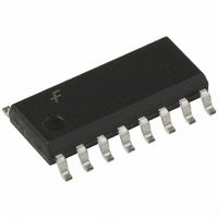
IC CROSSPOINT SWITCH 2X2 16SOIC
Manufacturer
Fairchild Semiconductor
Datasheet
1.FIN1022MX.pdf
(10 pages)
Specifications of FIN1022MX
Function
Crosspoint Switch
Circuit
1 x 2:2
On-state Resistance
75 Ohm
Voltage Supply Source
Single Supply
Voltage - Supply, Single/dual (±)
3 V ~ 3.6 V
Current - Supply
35mA
Operating Temperature
-40°C ~ 85°C
Mounting Type
Surface Mount
Package / Case
16-SOIC (0.154", 3.90mm Width)
Lead Free Status / RoHS Status
Lead free / RoHS Compliant
Other names
FIN1022MXTR
FIN1022MX_NL
FIN1022MX_NLTR
FIN1022MX_NLTR
FIN1022MX_NL
FIN1022MX_NLTR
FIN1022MX_NLTR
Available stocks
Company
Part Number
Manufacturer
Quantity
Price

Part Number:
FIN1022MX
Manufacturer:
FAIRCHILD/ن»™ç«¥
Quantity:
20 000


LVDS Differential Driver Characteristics
V
V
I
I
I
LVDS Differential Receiver Characteristics
V
V
V
I
LVTTL Control Characteristics
V
V
I
Device Characteristics
V
I
C
C
I
OZD
OFF
OS
IND
IN
PU/PD
CC
Absolute Maximum Ratings
DC Electrical Characteristics
Over supply voltage and operating temperature ranges, unless otherwise specified (Note 2)
Note 2: This part will only function with datasheet specification when a resistive load is applied to the driver outputs.
Note 3: All typical values are at T
V
V
Supply Voltage (V
DC Input Voltage (V
DC Output Voltage (V
Driver Short Circuit Current (I
Storage Temperature Range (T
Max Junction Temperature (T
Lead Temperature (T
OD
OS
TH
TL
IC
IH
IL
IK
IN
OUT
Symbol
OD
OS
(Soldering, 10 seconds)
Output Differential Voltage
V
Differential LOW-to-HIGH
Offset Voltage
Offset Magnitude Change from
Differential LOW-to-HIGH
Disabled Output Leakage Current
Power-Off Current
Short Circuit Output Current
Differential Input Threshold HIGH
Differential Input Threshold LOW
Input Common Mode Voltage
Input Current (Differential Inputs)
Input High Voltage
Input Low Voltage
Input Current
Input Clamp Voltage
Output Power-Up/Power-Down
High Z Leakage Current
Input Capacitance
Output Capacitance
Power Supply Current
OD
Magnitude Change from
CC
IN
)
L
)
OUT
)
Parameter
)
A
25 C and with V
OSD
J
)
STG
)
)
CC
65 C to 150 C
R
R
T
R
See Figure 3
See Figure 3
V
V
V
V
V
V
V
V
V
I
V
No Load, All Drivers Enabled
R
R
3.3V.
0.3V to 4.6V
0.3V to 4.6V
0.3V to 4.6V
IK
(Note 1)
A
L
L
L
OUT
CC
OUT
OUTx
IC
CC
IN
IN
IN
CC
L
L
Continuous
75 , See Figure 3
75 , See Figure 3
25 C and V
75 , See Figure 3
75 , All Drivers Enabled
75 , All Drivers Enabled
0.05V or 1.2V or 3.25V
GND
V
3.6V or GND
18 mA
0V, V
3.3V
0V to 1.5V
CC
3.6V or GND, Driver Disabled
0V, Driver Enabled
150 C
260 C
0V, V
IN
Test Conditions
or V
OUTx
CC
3
OUT
Recommended Operating
Conditions
Note 1: The “Absolute Maximum Ratings”: are those values beyond which
damage to the device may occur. The databook specifications should be
met, without exception, to ensure that the system design is reliable over its
power supply, temperature and output/input loading variables. Fairchild
does not recommend operation of circuits outside databook specification.
Supply Voltage (V
Input Voltage (V
Operating Temperature (T
Electrostatic Discharge
Electrostatic Discharge
3.3V
0V, Driver Enabled
(HBM 1.5 k , 100 pF)
(MM 0 , 100 pF)
3.6V or 0V
IN
)
CC
)
0.05
Min
270
285
1.0
100
1.5
2
A
)
(Note 3)
Typ
365
365
1.2
4.5
4.5
www.fairchildsemi.com
Max
1.45
3.25
475
440
100
0.8
35
35
35
35
35
10
20
10
10
20
20
20
10
40 C to 85 C
3.0V to 3.6V
0 to V
7500V
Units
300V
mV
mV
mV
mA
mV
mA
mA
mA
pF
pF
V
V
V
V
V
A
A
A
A
A
CC
Related parts for FIN1022MX
Image
Part Number
Description
Manufacturer
Datasheet
Request
R

Part Number:
Description:
Buffers & Line Drivers 3.3V LVDS Driver 1Bit HS Differential
Manufacturer:
Fairchild Semiconductor

Part Number:
Description:
Buffers & Line Drivers 3.3V Diff Driver LVDS 4Bit FT HS
Manufacturer:
Fairchild Semiconductor

Part Number:
Description:
Buffers & Line Drivers 3.3V Diff Driver LVDS 4Bit FT HS
Manufacturer:
Fairchild Semiconductor

Part Number:
Description:
Fairchild Semiconductor [IGBT MODULE]
Manufacturer:
Fairchild Semiconductor
Datasheet:

Part Number:
Description:
Discrete Semiconductor Modules
Manufacturer:
Fairchild Semiconductor
Part Number:
Description:
Discrete Semiconductor Modules
Manufacturer:
Fairchild Semiconductor
Part Number:
Description:
This N-Channel MOSFET is produced using Fairchild Semiconductor’s advanced Power Trench® process
Manufacturer:
Fairchild Semiconductor
Datasheet:
Part Number:
Description:
This N-Channel MOSFET is produced using Fairchild Semiconductor’s advanced Power Trench® process
Manufacturer:
Fairchild Semiconductor
Datasheet:
Part Number:
Description:
This N-Channel MOSFET is produced using Fairchild Semiconductor’s advanced PowerTrench® process
Manufacturer:
Fairchild Semiconductor
Datasheet:
Part Number:
Description:
This N-Channel MOSFET is produced using Fairchild Semiconductor’s advanced PowerTrench® process
Manufacturer:
Fairchild Semiconductor
Datasheet:
Part Number:
Description:
This N-Channel MOSFET is produced using Fairchild Semiconductor’s advanced Power Trench® process
Manufacturer:
Fairchild Semiconductor
Datasheet:
Part Number:
Description:
This N-Channel logic Level MOSFETs are produced using Fairchild Semiconductor‘s advanced Power Trench® process that has been special tailored to minimize the on-state resistance and yet maintain superior switching performance
Manufacturer:
Fairchild Semiconductor
Datasheet:
Part Number:
Description:
This N-Channel MOSFET is produced using Fairchild Semiconductor’s advanced Power Trench® process
Manufacturer:
Fairchild Semiconductor
Datasheet:
Part Number:
Description:
This N-Channel SyncFET™ is produced using Fairchild Semiconductor’s advanced PowerTrench® process
Manufacturer:
Fairchild Semiconductor
Datasheet:
Part Number:
Description:
This N-Channel SyncFET™ is produced using Fairchild Semiconductor’s advanced PowerTrench® process
Manufacturer:
Fairchild Semiconductor
Datasheet: