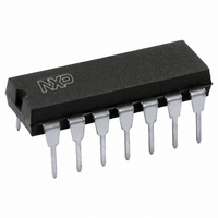
HEF4066BP,652 NXP Semiconductors, HEF4066BP,652 Datasheet - Page 6

HEF4066BP,652
Manufacturer Part Number
HEF4066BP,652
Description
IC SWITCH QUAD 1X1 14DIP
Manufacturer
NXP Semiconductors
Series
4000Br
Type
Analog Switchr
Specifications of HEF4066BP,652
Package / Case
14-DIP (0.300", 7.62mm)
Function
Switch
Circuit
4 x 1:1
On-state Resistance
175 Ohm
Voltage Supply Source
Dual Supply
Voltage - Supply, Single/dual (±)
±3 V ~ 15 V
Current - Supply
4µA
Operating Temperature
-40°C ~ 85°C
Mounting Type
Through Hole
Switch Configuration
SPST
On Resistance (max)
2500 Ohm @ 5 V
On Time (max)
90 ns @ 5 V
Off Time (max)
160 ns @ 5 V
Supply Voltage (max)
15.5 V
Supply Voltage (min)
4.5 V
Maximum Power Dissipation
100 mW
Maximum Operating Temperature
+ 85 C
Mounting Style
Through Hole
Minimum Operating Temperature
- 40 C
Propagation Delay Time
5 ns
Package
14PDIP
Maximum On Resistance
2500@5V Ohm
Maximum Propagation Delay Bus To Bus
20@5V|10@10V|10@15V ns
Maximum Low Level Output Current
10 mA
Maximum Turn-off Time
160@5V ns
Maximum Turn-on Time
90@5V ns
Switch Architecture
SPST
Power Supply Type
Single
Lead Free Status / RoHS Status
Lead free / RoHS Compliant
Lead Free Status / RoHS Status
Lead free / RoHS Compliant, Lead free / RoHS Compliant
Other names
568-1694-5
933296650652
HEF4066BPN
933296650652
HEF4066BPN
NXP Semiconductors
11. Dynamic characteristics
Table 8.
T
Table 9.
P
HEF4066B_6
Product data sheet
Symbol
t
t
t
t
t
Symbol
P
PHL
PHZ
PZH
PLZ
PZL
amb
D
D
can be calculated from the formulas shown; V
= 25
°
C; V
Parameter
HIGH to LOW propagation delay nY, nZ to nZ, nY; see
HIGH to OFF-state
propagation delay
OFF-state to HIGH
propagation delay
LOW to OFF-state
propagation delay
OFF-state to LOW
propagation delay
Dynamic characteristics
Dynamic power dissipation P
Parameter
dynamic power
dissipation
SS
= 0 V; for test circuit see
V
10 V
15 V
5 V
DD
All information provided in this document is subject to legal disclaimers.
Typical formula for P
P
P
P
Figure
D
D
D
D
Conditions
nY, nZ to nZ, nY; see
nE to nY, nZ; see
nE to nY, nZ; see
nE to nY, nZ; see
nE to nY, nZ; see
= 2500 × f
= 11500 × f
= 29000 × f
SS
Rev. 06 — 25 March 2010
9.
= 0 V; t
i
+ Σ(f
i
i
+ Σ(f
+ Σ(f
r
= t
o
f
o
o
Figure 8
Figure 8
Figure 8
Figure 8
× C
≤
× C
× C
D
20 ns; T
(μW)
Figure 7
Figure 7
L
) × V
L
L
) × V
) × V
Quad single-pole single-throw analog switch
DD
amb
DD
DD
2
2
2
= 25
°
C.
V
10 V
15 V
10 V
15 V
10 V
15 V
10 V
15 V
10 V
15 V
10 V
15 V
where:
f
f
C
V
Σ(C
5 V
5 V
5 V
5 V
5 V
5 V
DD
i
o
DD
= input frequency in MHz;
L
= output frequency in MHz;
= output load capacitance in pF;
L
= supply voltage in V;
× f
o
) = sum of the outputs.
Typ
10
5
5
10
5
5
80
65
60
40
20
15
80
70
70
45
20
15
HEF4066B
© NXP B.V. 2010. All rights reserved.
Max
20
10
10
20
10
10
160
130
120
80
40
30
160
140
140
90
40
30
Unit
ns
ns
ns
ns
ns
ns
ns
ns
ns
ns
ns
ns
ns
ns
ns
ns
ns
ns
6 of 16


