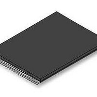
S29GL256S10TFI010 Spansion Inc., S29GL256S10TFI010 Datasheet - Page 10

S29GL256S10TFI010
Manufacturer Part Number
S29GL256S10TFI010
Description
Flash 256 MBIT 3V 100NS PAGE MODE FLASH
Manufacturer
Spansion Inc.
Datasheet
1.S29GL256S10TFI010.pdf
(97 pages)
Specifications of S29GL256S10TFI010
Data Bus Width
16 bit
Memory Type
Flash
Memory Size
256 Mbit
Architecture
Uniform
Timing Type
Asynchronous
Interface Type
CFI
Access Time
100 ns
Supply Voltage (max)
3.6 V
Supply Voltage (min)
2.7 V
Maximum Operating Current
100 mA
Operating Temperature
- 40 C to + 85 C
Mounting Style
SMD/SMT
Package / Case
TSOP-56
Lead Free Status / Rohs Status
Compliant
Available stocks
Company
Part Number
Manufacturer
Quantity
Price
Company:
Part Number:
S29GL256S10TFI010
Manufacturer:
Spansion
Quantity:
25
1.
10
Product Overview
The GL-S family consists of 128-Mbit to 1Gbit, 3.0V core, Versatile I/O, non-volatile, flash memory devices.
These devices have a 16-bit (word) wide data bus and use only word boundary addresses. All read accesses
provide 16 bits of data on each bus transfer cycle. All writes take 16 bits of data from each bus transfer cycle.
:
Note:
** A
The GL-S family combines the best features of eXecute In Place (XIP) and Data Storage flash memories.
This family has the fast random access of XIP flash along with the high density and fast program speed of
Data Storage flash.
Read access to any random location takes 90 ns to 120 ns depending on device density and I/O power
supply voltage. Each random (initial) access reads an entire 32-byte aligned group of data called a Page.
Other words within the same Page may be read by changing only the low order 4 bits of word address. Each
access within the same Page takes 15 ns to 30 ns. This is called Page Mode read. Changing any of the
higher word address bits will select a different Page and begin a new initial access. All read accesses are
asynchronous.
A
Max
Max
RESET#
**–A0
GL01GS = A25, A
WE#
WP#
OE#
V
CE#
V
V
CC
SS
IO
RY/BY#
Max
V
CC
Command
Register
Control
GL512S = A24, A
State
D a t a
Detector
S h e e t
GL-S MirrorBit
Max
GL256S = A23, A
PGM Voltage
Figure 1.1 Block Diagram
Generator
Timer
( A d v a n c e
®
Family
Sector Switches
Erase Voltage
Max
Generator
GL128S = A22
STB
I n f o r m a t i o n )
S29GL_128S_01GS_00_01 February 11, 2011
Output Enable
Chip Enable
Logic
Y-Decoder
X-Decoder
STB
DQ15
Input/Output
Buffers
Cell Matrix
Y-Gating
Latch
Data
–
DQ0


