DG441DY Intersil, DG441DY Datasheet - Page 4
DG441DY
Manufacturer Part Number
DG441DY
Description
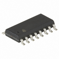
IC SWITCH QUAD SPST 16SOIC
Manufacturer
Intersil
Datasheet
1.DG441DY.pdf
(14 pages)
Specifications of DG441DY
Function
Switch
Circuit
4 x SPST - NO
On-state Resistance
85 Ohm
Voltage Supply Source
Single, Dual Supply
Voltage - Supply, Single/dual (±)
5 V ~ 34 V, ±5 V ~ 22 V
Operating Temperature
-40°C ~ 85°C
Mounting Type
Surface Mount
Package / Case
16-SOIC (0.154", 3.90mm Width)
Lead Free Status / RoHS Status
Contains lead / RoHS non-compliant
Other names
DG441DYIS
Available stocks
Company
Part Number
Manufacturer
Quantity
Price

Part Number:
DG441DY
Manufacturer:
VISHAY/威世
Quantity:
20 000
Company:
Part Number:
DG441DY+
Manufacturer:
Intersil
Quantity:
47
Part Number:
DG441DY-E3
Manufacturer:
VISHAY/威世
Quantity:
20 000
Company:
Part Number:
DG441DY-T
Manufacturer:
INTERSIL
Quantity:
2 500
Company:
Part Number:
DG441DY-T1
Manufacturer:
SHARP
Quantity:
41 960
Part Number:
DG441DY-T1
Manufacturer:
SILICONIX
Quantity:
20 000
Part Number:
DG441DY-T1-E
Manufacturer:
VISHAY/威世
Quantity:
20 000


Absolute Maximum Ratings
V+ to V- . . . . . . . . . . . . . . . . . . . . . . . . . . . . . . . . . . . . . . . . . . 44.0V
GND to V-. . . . . . . . . . . . . . . . . . . . . . . . . . . . . . . . . . . . . . . . . . -25V
GND to V+ . . . . . . . . . . . . . . . . . . . . . . . . . . . . . . . . . . . . . . . . .+34V
Digital Inputs, V
Continuous Current (Any Terminal) . . . . . . . . . . . . . . . . . . . . . 30mA
Peak Current, S or D (Pulsed 1ms, 10% Duty Cycle Max) . . 100mA
Operating Conditions
Temperature Range . . . . . . . . . . . . . . . . . . . . . . . . . .-40°C to +85°C
Signal Voltage Range . . . . . . . . . . . . . . . . . . . . . . . . . . . . . . ±20V (Max)
Input Low Voltage . . . . . . . . . . . . . . . . . . . . . . . . . . . . . . 0.8V (Max)
Input High Voltage . . . . . . . . . . . . . . . . . . . . . . . . . . . . . . 2.4V (Min)
Input Rise and Fall Time . . . . . . . . . . . . . . . . . . . . . . . . . . . . . . . . .≤20ns
CAUTION: Stresses above those listed in “Absolute Maximum Ratings” may cause permanent damage to the device. This is a stress only rating and operation of the
device at these or any other conditions above those indicated in the operational sections of this specification is not implied.
NOTES:
Electrical Specifications
DYNAMIC CHARACTERISTICS
Turn-ON Time, t
Turn-OFF Time, t
Charge Injection, Q (Figure 2)
OFF Isolation (Figure 4)
Crosstalk (Channel-to-Channel) (Figure 3)
Source OFF Capacitance, C
Drain OFF Capacitance, C
Channel ON Capacitance,
C
DIGITAL INPUT CHARACTERISTICS
Input Current V
Input Current V
ANALOG SWITCH CHARACTERISTICS
Analog Signal Range, V
Drain-Source ON Resistance, r
Source OFF Leakage Current, I
Drain OFF Leakage Current, I
Channel ON Leakage Current,
I
1. Signals on S
2. θ
D(ON)
D(ON)
. . . . . . . . (V-) -2V to (V+) + 2V or 30mA, Whichever Occurs First
DG441
DG442
JA
+ I
is measured with the component mounted on a high effective thermal conductivity test board in free air. See Tech Brief TB379 for details.
+ C
S(ON)
S(ON)
PARAMETER
S
IN
IN
X
ON
, V
OFF
, D
Low, I
High, I
D
X
(Note 1)
or IN
IL
ANALOG
IH
D(OFF)
X
S(OFF)
exceeding V+ or V- will be clamped by internal diodes. Limit forward diode current to maximum current ratings.
D(OFF)
DS(ON
S(OFF)
4
(Dual Supply) Test Conditions: V+ = +15V, V- = -15V, V
Unless Otherwise Specified
)
R
C
R
f = 1MHz, V
V
V
I
V- = -13.5V
V+ = 16.5V, V- = -16.5V, V
V
V+ = 16.5V, V- = -16.5V, V
S
L
IN
IN
S
L
L
=
= 1nF, V
= 1kΩ, C
= 50Ω, C
=
Under Test = 0.8V, All Others = 2.4V
Under Test = 2.4V, All Others = 0.8V
10mA, V
15.5V
G
ANALOG
L
TEST CONDITIONS
L
= 0V, R
= 35pF, V
= 5pF, f = 1MHz
D
DG441, DG442
= ±8.5V, V+ = 13.5V,
G
= 0 (Figure 5)
= 0Ω
S
= ±10V, (Figure 1)
D
S
= ±15.5V,
= V
D
Thermal Information
Thermal Resistance (Typical, Note 2)
Maximum Junction Temperature (Plastic Packages) . . . . . . +150°C
Maximum Storage Temperature Range . . . . . . . . . .-65°C to +150°C
Maximum Lead Temperature (Soldering 10s) . . . . . . . . . . . +300°C
*Pb-free PDIPs can be used for through hole wave solder
processing only. They are not intended for use in Reflow solder
processing applications.
= ±15.5V
PDIP Package* . . . . . . . . . . . . . . . . . . . . . . . . . . . .
SOIC Package . . . . . . . . . . . . . . . . . . . . . . . . . . . . .
TSSOP Package . . . . . . . . . . . . . . . . . . . . . . . . . . .
(SOIC and TSSOP- Lead Tips Only)
IN
= 2.4V, 0.8V, V
TEMP
(°C)
+25
+25
+25
+25
+25
+25
+25
+25
Full
Full
Full
+25
+85
+25
+85
+25
+85
+25
+85
MIN
-0.5
-0.5
-0.5
-0.5
-0.5
-15
-10
-5
-5
-
-
-
-
-
-
-
-
-
-
-
ANALOG
(NOTE 3)
-0.00001
0.00001
= V
TYP
-100
0.01
0.01
0.08
150
110
90
60
16
50
-1
4
4
-
-
-
-
-
S
, V
D
,
MAX
250
120
210
100
0.5
0.5
0.5
0.5
0.5
85
15
10
5
5
-
-
-
-
-
-
November 20, 2006
θ
JA
FN3281.10
UNITS
115
150
(°C/W)
90
pC
dB
μA
μA
dB
pF
pF
pF
nA
nA
nA
nA
nA
nA
ns
ns
ns
V
Ω
Ω
Related parts for DG441DY
Image
Part Number
Description
Manufacturer
Datasheet
Request
R

Part Number:
Description:
Monolithic Quad SPST CMOS Analog Switches
Manufacturer:
INTERSIL [Intersil Corporation]
Datasheet:

Part Number:
Description:
Intersil Corporation [CMOS Serial Controller Interface]
Manufacturer:
Intersil Corporation
Datasheet:
Part Number:
Description:
Manufacturer:
Intersil Corporation
Datasheet:
Part Number:
Description:
357-036-542-201 CARDEDGE 36POS DL .156 BLK LOPRO
Manufacturer:
Intersil Corporation
Datasheet:
Part Number:
Description:
1024-Word x 4-Bit LSI Static RAM
Manufacturer:
Intersil Corporation
Datasheet:
Part Number:
Description:
General Purpose NPN Transistor Arrays FN341.4
Manufacturer:
Intersil Corporation
Datasheet:
Part Number:
Description:
CMOS 16-Bit Microprocessor
Manufacturer:
Intersil Corporation
Datasheet:
Part Number:
Description:
Manufacturer:
Intersil Corporation
Datasheet:
Part Number:
Description:
Manufacturer:
Intersil Corporation
Datasheet:
Part Number:
Description:
Manufacturer:
Intersil Corporation
Datasheet:
Part Number:
Description:
Manufacturer:
Intersil Corporation
Datasheet:
Part Number:
Description:
CMOS 6-Bit Latch and Decoder Memory Interfaces
Manufacturer:
Intersil Corporation
Datasheet:
Part Number:
Description:
CA3046General Purpose NPN Transistor Arrays
Manufacturer:
Intersil Corporation
Datasheet:
Part Number:
Description:
Manufacturer:
Intersil Corporation
Datasheet:
Part Number:
Description:
TR909 DLC/FLC SLIC with Low Power Standby
Manufacturer:
Intersil Corporation
Datasheet: