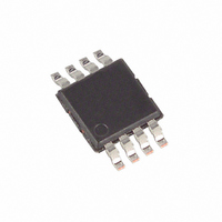
DG418LEUA+ Maxim Integrated Products, DG418LEUA+ Datasheet - Page 6

DG418LEUA+
Manufacturer Part Number
DG418LEUA+
Description
IC SWITCH SPST 8UMAX
Manufacturer
Maxim Integrated Products
Type
Analog Switchr
Specifications of DG418LEUA+
Function
Switch
Circuit
1 x SPST- NO
On-state Resistance
35 Ohm
Voltage Supply Source
Single, Dual Supply
Voltage - Supply, Single/dual (±)
10 V ~ 30 V, ±4.5 V ~ 20 V
Mounting Type
Surface Mount
Package / Case
8-TSSOP, 8-MSOP (0.118", 3.00mm Width)
Number Of Switches
Dual
Switch Configuration
SPST
On Resistance (max)
35 Ohms
On Time (max)
175 ns
Off Time (max)
185 ns
Off Isolation (typ)
- 90 dB
Supply Voltage (max)
+/- 20 V
Supply Voltage (min)
+/- 4.5 V
Supply Current
26 uA
Maximum Power Dissipation
362 mW
Maximum Operating Temperature
+ 85 C
Mounting Style
SMD/SMT
Description/function
Analog Switch
Input Level
CMOS, TTL
Minimum Operating Temperature
- 40 C
Off State Leakage Current (max)
5 nA
Package
8uSOP
Maximum On Resistance
100@10.8V Ohm
Maximum Low Level Output Current
30 mA
Maximum Turn-off Time
210@12V ns
Maximum Turn-on Time
300@12V ns
Switch Architecture
SPST
Power Supply Type
Single|Dual
Lead Free Status / RoHS Status
Lead free / RoHS Compliant
Using supply voltages other than ±15V reduces the
analog signal range. The DG417/DG418/DG419 switch-
es operate with ±4.5V to ±20V bipolar supplies or with
a +10V to +30V single supply; connect V- to 0V when
operating with a single supply. Also, all device types
can operate with unbalanced supplies, such as +24V
and -5V. VL must be connected to +5V to be TTL com-
patible, or to V+ for CMOS-logic level inputs. The
Typical Operating Characteristics graphs show typical
on-resistance with ±20V, ±15V, ±10V, and ±5V sup-
plies. (Switching times increase by a factor of two or
more for operation at ±5V.)
Proper power-supply sequencing is recommended for
all CMOS devices. Do not exceed the absolute maxi-
mum ratings because stresses beyond the listed rat-
ings may cause permanent damage to the devices.
Always sequence V+ on first, followed by VL, V-, and
logic inputs. If power-supply sequencing is not possi-
ble, add two small, external signal diodes in series with
the supply pins for overvoltage protection (Figure 1).
Improved, SPST/SPDT Analog Switches
6
______________________________________________________________Pin Description
__________Applications Information
DG417
_______________________________________________________________________________________
—
—
—
1
2
3
4
5
6
7
8
DG418
PIN
—
—
—
1
2
3
4
5
6
7
8
Operation with Supply Voltages
DG419
—
—
—
2
3
4
5
6
7
1
8
Overvoltage Protection
NAME
GND
N.C.
S1
V+
VL
S2
IN
V-
D
S
S
Other than ±15V
Analog-Switch Source Terminal (normally closed)
Analog-Switch Source Terminal (normally open)
Analog-Switch Source Terminal 1 (normally closed)
No Internal Connection
Logic Ground
Analog-Signal Positive Supply Input
Logic-Level Positive Supply Input
Logic-Level Input
Analog-Signal Negative Supply Input
Analog-Switch Drain Terminal
Analog-Switch Source Terminal 2 (normally open)
Adding diodes reduces the analog signal range to 1V
below V+ and 1V above V-, without affecting low switch
resistance and low leakage characteristics. Device
operation is unchanged, and the difference between
V+ and V- should not exceed +44V.
Figure 1. Overvoltage Protection Using External Blocking Diodes
V
g
FUNCTION
S
V+
V-
DG41_
D


