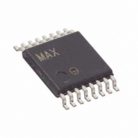
MAX4651EUE+ Maxim Integrated Products, MAX4651EUE+ Datasheet - Page 8

MAX4651EUE+
Manufacturer Part Number
MAX4651EUE+
Description
IC SWITCH QUAD SPST 16TSSOP
Manufacturer
Maxim Integrated Products
Datasheet
1.MAX4651EUE.pdf
(15 pages)
Specifications of MAX4651EUE+
Function
Switch
Circuit
4 x SPST - NC
On-state Resistance
4 Ohm
Voltage Supply Source
Single Supply
Voltage - Supply, Single/dual (±)
1.8 V ~ 5.5 V
Current - Supply
1µA
Operating Temperature
-40°C ~ 85°C
Mounting Type
Surface Mount
Package / Case
16-TSSOP
Number Of Switches
Quad
Switch Configuration
SPDT
On Resistance (max)
4 Ohms
On Time (max)
14 ns
Off Time (max)
8 ns
Off Isolation (typ)
- 75 dB
Supply Voltage (max)
5.5 V
Supply Voltage (min)
1.8 V
Supply Current
0.001 uA
Maximum Power Dissipation
457 mW
Maximum Operating Temperature
+ 85 C
Mounting Style
SMD/SMT
Description/function
Analog Switch
Input Level
CMOS, TTL
Minimum Operating Temperature
- 40 C
Off State Leakage Current (max)
0.1 nA
Lead Free Status / RoHS Status
Lead free / RoHS Compliant
Low-Voltage, 4Ω, Quad, SPST,
CMOS Analog Switches
The MAX4651/MAX4652/MAX4653 are low on-resis-
tance, low-voltage analog switches that operate from a
single +1.8V to +5.5V supply. CMOS switch construc-
tion allows processing analog signals that are within the
supply voltage range (GND to V+).
Proper power-supply sequencing is recommended for
all CMOS devices. Do not exceed the absolute maxi-
mum ratings because stresses beyond the listed rat-
ings can cause permanent damage to the devices.
Always sequence V+ on first, followed by the logic
inputs, NO or COM. If power-supply sequencing is not
possible, add two small signal diodes (D1, D2) in series
with the supply pins for overvoltage protection (Figure
1). Adding these diodes reduces the analog signal by
one diode drop below V+ and one diode drop above
GND, but does not affect the devices’ low switch resis-
tance and low leakage characteristics. Device opera-
tion is unchanged, and the difference between V+ and
GND should not exceed 6V.
Although it is not required, power-supply bypassing
improves noise margin and prevents switching noise
from propagating from the V+ supply to other compo-
nents. A 0.1µF capacitor connected from V+ to GND is
adequate for most applications.
8
________________________________________________________________________________________
Applications Information
Detailed Description
Figure 1. Overvoltage Protection Using External Blocking
Diodes
TRANSISTOR COUNT: 205
* INTERNAL PROTECTION DIODES
COM_
*
*
GND
V+
V+
Chip Information
D1
D2
*
*
MAX4651
MAX4652
MAX4653
NO_


