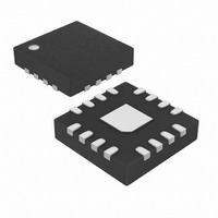
MAX4899AEETE+ Maxim Integrated Products, MAX4899AEETE+ Datasheet - Page 10

MAX4899AEETE+
Manufacturer Part Number
MAX4899AEETE+
Description
IC MULTIPLEXER DUAL 4X1 16TQFN
Manufacturer
Maxim Integrated Products
Datasheet
1.MAX4899EETE.pdf
(14 pages)
Specifications of MAX4899AEETE+
Function
Multiplexer
Circuit
2 x 4:1
On-state Resistance
12 Ohm
Voltage Supply Source
Single Supply
Voltage - Supply, Single/dual (±)
2.7 V ~ 3.6 V
Current - Supply
3µA
Operating Temperature
-40°C ~ 85°C
Mounting Type
Surface Mount
Package / Case
16-WFQFN Exposed Pad
Lead Free Status / RoHS Status
Lead free / RoHS Compliant
USB 2.0 High-Speed, Fault-Tolerant 3:1, 4:1
Multiplexers
The MAX4899E/MAX4899AE analog multiplexers com-
bine the low on-capacitance (C
tance (R
applications. These devices are designed for USB 2.0
high-speed applications at 480Mbps. The MAX4899E/
MAX4899AE also handle all the requirements for USB
low- and full-speed signaling. In the case of USB low/
full speed, these devices can function normally even if
the supply voltage is 2.7V, even though the USB signal
may be higher than the supply voltage.
The MAX4899E is a dual 3:1 multiplexer, whereas the
MAX4899AE is a dual 4:1 multiplexer. The MAX4899E/
MAX4899AE feature two digital inputs, C
trol the analog signal path. Typical applications include
switching a USB connector between USB and other oper-
ations such as serial communications, audio, and video.
An enable input (EN) is provided to disable all channels
and place the device into a high-impedance (off) state,
as well as shutting off the charge pump for minimum
power consumption. The MAX4899E/MAX4899AE fea-
ture an additional charge-pump enable input (QP) to
disable the charge pump. The switches remain active
at a lower analog signal range and higher R
The MAX4899E/MAX4899AE operate from a 2.7V to
3.6V power-supply voltage and are current-limit pro-
tected against +5.5V shorts to COM
The MAX4899E/MAX4899AE provide two digital control
inputs (C
between the COM
tables for the MAX4899E/MAX4899AE are shown in the
Functional Diagrams. Since the MAX4899E only has
three USB__ channels, the code C
used to place all channels into a high-impedance state.
This is particularly useful for eliminating the extra con-
trol line to the EN input that is normally used for dis-
abling all channels. Driving C
minimizes power consumption.
The MAX4899E/MAX4899AE feature an enable input
(EN) that when driven high places all channels into a
high-impedance state, as an all-off feature. The internal
charge pump is also disabled when EN is high, thus
minimizing the quiescent supply current. For normal
operation, drive EN low.
The charge-pump input (QP) disables and enables the
internal charge pump. Drive QP high to disable the
charge pump and reduce the quiescent supply current.
10
______________________________________________________________________________________
ON
0
) necessary for high-performance switching
, C
Charge-Pump Enable Input ( QP )
1
) to select the analog signal path
Digital Control Inputs (C
A
_ and USB__ channels. The truth
Detailed Description
ON
Enable Input ( EN )
0
A
) and low on-resis-
and C
1
- and COM
:C
0
0
and C
= 1:1 can be
1
ON
rail-to-rail
1
.
, to con-
A
0
+.
, C
1
)
With the charge pump disabled, the MAX4899E/
MAX4899AE still function normally; however, the analog
signal range is reduced and the switch on-resistance
(R
charge pump disabled is 0V to 1.5V. For normal opera-
tion, drive QP low.
Signals applied to COM
minals, and signals applied to COM
USB_- terminals. These multiplexers are bidirectional,
allowing COM
inputs or outputs. The D+ and D- notation in the Pin
Description table is arbitrary and can be interchanged.
For example, USB D+ signals can be applied to COM
and are routed to the USB_- terminals. Additionally,
these multiplexers can be used for non-USB signals.
COM
circuitry and are ±15kV ESD protected.
The MAX4899E is a dual 3:1 multiplexer, allowing
COM
and COM
The MAX4899AE is a dual 4:1 multiplexer, allowing
COM
COM
The MAX4899E/MAX4899AE feature +5.5V fault protec-
tion to COM
between 4.5V to 5.5V, the switch automatically goes
into a current-limiting mode that limits current to less
than 2mA. Fault protection prevents these switches and
downstream devices from being damaged due to
shorts to the USB bus voltage rail.
The MAX4899E/MAX4899AE analog multiplexers are
fully compliant with the USB 2.0 specification. The low
on-resistance and low on-capacitance of these multi-
plexers make them ideal for high-performance switch-
ing applications. The MAX4899E/MAX4899AE are ideal
for routing USB data lines and for applications that
require switching between different data types (see
Figure 8).
High-speed switches require proper layout and design
procedures for optimum performance. Keep design-
controlled impedance PC board traces as short as pos-
sible. Ensure that bypass capacitors are placed as
close to the device as possible and use large ground
planes where possible.
ON
A
A
A
A
) is increased. The analog signal range with the
+ and COM
+ to be routed to one of four USB_+ channels, and
- to be routed to one of four USB_- channels.
+ to be routed to one of three USB_+ channels,
A
- to be routed to one of three USB_- channels.
A
A
+ and COM
_ and USB_ to be configured as either
Applications Information
Overvoltage Fault Protection
A
- are normally connected to outside
A
+ are routed to the USB_+ ter-
Analog Signal Levels
A
-. When a fault occurs
A
USB Switching
- are routed to the
Board Layout
A
-


