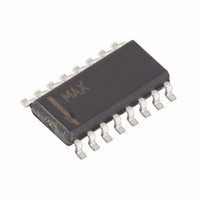
MAX4546CSE+ Maxim Integrated Products, MAX4546CSE+ Datasheet - Page 10

MAX4546CSE+
Manufacturer Part Number
MAX4546CSE+
Description
IC VIDEO SWITCH DUAL SPST 16SOIC
Manufacturer
Maxim Integrated Products
Datasheet
1.MAX4546CSE.pdf
(16 pages)
Specifications of MAX4546CSE+
Function
Video Switch
Circuit
2 x SPST - NC/NO
On-state Resistance
20 Ohm
Voltage Supply Source
Single, Dual Supply
Voltage - Supply, Single/dual (±)
2.7 V ~ 12 V, ± 2.7 V ~ 6 V
Current - Supply
1µA
Operating Temperature
0°C ~ 70°C
Mounting Type
Surface Mount
Package / Case
16-SOIC (0.154", 3.90mm Width)
Lead Free Status / RoHS Status
Lead free / RoHS Compliant
Single-supply operation also limits signal levels and
interferes with grounded signals. When V- = 0V, AC sig-
nals are limited to -0.3V. Voltages below -0.3V can be
clipped by the internal ESD-protection diodes, and the
parts can be damaged if excessive current flows.
When power to the MAX4545/MAX4546/MAX4547 is off
(i.e., V+ = 0V and V- = 0V), the Absolute Maximum
Ratings still apply. This means that neither logic-level
inputs on IN_ nor signals on COM_, NO_, or NC_ can
exceed ±0.3V. Voltages beyond ±0.3V cause the inter-
nal ESD-protection diodes to conduct, and the parts
can be damaged if excessive current flows.
Satisfactory high-frequency operation requires that
careful consideration be given to grounding. For most
applications, a ground plane is strongly recom-
mended, and all GND_ pins should be connected to
it with solid copper. While the V+ and V- power-supply
pins are common to all switches in a given package,
each switch has separate ground pins that are not
internally connected to each other. This contributes to
the overall high-frequency performance and provides
added flexibility in some applications, but it can cause
problems if it is overlooked. All the GND_ pins have
ESD diodes to V+ and V-.
In systems that have separate digital and analog (sig-
nal) grounds, connect these switch GND_ pins to ana-
log ground. Preserving a good signal ground is much
more important than preserving a digital ground.
Ground current is only a few nanoamps.
The logic-level inputs, IN_, have voltage thresholds
determined by V+ and GND_. (V- does not influence
the logic-level threshold.) With +5V and 0V applied to
V+ and GND_, the threshold is about 1.6V, ensuring
compatibility with TTL- and CMOS-logic drivers.
The various GND_ pins can be connected to separate
voltage potentials if any or all of the logic-level inputs is
not a normal logic signal. (The GND_ voltages cannot
exceed (V+ - 2V) or V-.) Elevating GND_ reduces off
isolation. For example, using the MAX4545, if GND2–
GND6 are connected to 0V and GND1 is connected to
V-, then switches 2, 3, and 4 would be TTL/CMOS com-
patible, but switch 1 (IN1) could be driven with the rail-
to-rail output of an op amp operating from V+ and V-.
Note, however, that IN_ can be driven more negative
than GND_, as far as V-. GND_ does not have to be
removed from 0V when IN_ is driven from bipolar
sources, but the voltage on IN_ should never exceed V-.
Quad/Dual, Low-Voltage,
Bidirectional RF/Video Switches
10
______________________________________________________________________________________
DC Ground Considerations
Grounding
Power Off
GND_ should be separated from 0V only if the logic-
level threshold has to be changed.
Any GND_ pin not connected to 0V should be
bypassed to the ground plane with a surface-mount
10nF capacitor to maintain good RF grounding. DC
current in the IN_ and GND_ pins is less than 1nA, but
increases with switching frequency.
On the MAX4545 only, two extra ground pins—GND5
and GND6—are provided to improve isolation and
crosstalk. They are not connected to the logic-level cir-
cuit. These pins should always be connected to the
ground plane with solid copper.
A ground plane is mandatory for satisfactory high-
frequency operation. (Prototyping using hand wiring or
wire-wrap boards is strongly discouraged.) Connect all
0V GND_ pins to the ground plane with solid copper.
(The GND_ pins extend the high-frequency ground
through the package wire-frame, into the silicon itself,
thus improving isolation.) The ground plane should be
solid metal underneath the device, without interruptions.
There should be no traces under the device itself. For
DIP packages, this applies to both sides of a two-sided
board. Failure to observe this will have a minimal effect
on the “on” characteristics of the switch at high frequen-
cies, but it will degrade the off isolation and crosstalk.
All V+ and V- pins should be bypassed to the ground
plane with surface-mount 10nF capacitors. For DIP
packages, they should be mounted as close as possi-
ble to the pins on the same side of the board as the
device. Do not use feedthroughs or vias for bypass
capacitors. For surface-mount packages, the pins are
so close to each other that the bypass capacitors
should be mounted on the opposite side of the board
from the device. In this case, use short feedthroughs or
vias, directly under the V+ and V- pins. Any GND_ pin
not connected to 0V should be similarly bypassed. If V-
is 0V, connect it directly to the ground plane with solid
copper. Keep all leads short.
The MAX4547 has two V+ and V- pins. Make DC con-
nections to only one of each to minimize crosstalk. Do
not route DC current into one of the V+ or V- pins and
out the other V+ or V- pin to other devices. The second
set of V+ and V- pins is for AC bypassing only.
For dual-supply operation, the MAX4547 should have
four 10nF bypass capacitors connected to each V+
and V- pin, as close to the package as possible. For
single-supply operation, the MAX4547 should have two
10nF bypass capacitors connected (one to each V+
pin), as close to the package as possible.
AC Ground and Bypassing


