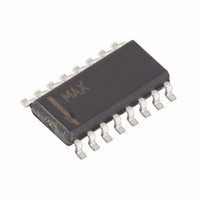
MAX4622ESE+ Maxim Integrated Products, MAX4622ESE+ Datasheet - Page 7

MAX4622ESE+
Manufacturer Part Number
MAX4622ESE+
Description
IC SWITCH DUAL SPST 16SOIC
Manufacturer
Maxim Integrated Products
Type
Analog Switchr
Datasheet
1.MAX4622CPE.pdf
(12 pages)
Specifications of MAX4622ESE+
Function
Switch
Circuit
2 x SPST - NC/NO
On-state Resistance
5 Ohm
Voltage Supply Source
Single, Dual Supply
Voltage - Supply, Single/dual (±)
4.5 V ~ 36 V, ±4.5 V ~ 18 V
Operating Temperature
-40°C ~ 85°C
Mounting Type
Surface Mount
Package / Case
16-SOIC (0.154", 3.90mm Width)
Package
16SOIC N
Maximum On Resistance
8@12V Ohm
Maximum Low Level Output Current
100 mA
Number Of Channels Per Chip
2
Maximum Turn-off Time
200@±15V ns
Maximum Turn-on Time
350@12V ns
Switch Architecture
SPDT
Power Supply Type
Single|Dual
Number Of Switches
Dual
Switch Configuration
SPDT
On Resistance (max)
5 Ohms
On Time (max)
250 ns
Off Time (max)
200 us
Off Isolation (typ)
- 62 dB
Supply Voltage (max)
+/- 20 V
Supply Voltage (min)
+/- 4.5 V
Supply Current
0.001 uA
Maximum Power Dissipation
696 mW
Maximum Operating Temperature
+ 85 C
Mounting Style
SMD/SMT
Description/function
Analog Switch
Input Level
CMOS, TTL
Minimum Operating Temperature
- 40 C
Off State Leakage Current (max)
0.5 nA
Lead Free Status / RoHS Status
Lead free / RoHS Compliant
MAX4621
MAX4622
MAX4623
4, 5, 9, 16
4, 5, 9, 16
1, 3, 6, 8
1, 3, 6, 8
10, 15
10, 15
10, 15
9, 16
PIN
1, 8
2–7
2, 7
2, 7
11
12
13
14
11
12
13
14
11
12
13
14
NO2, NO1
NC_, NO_
IN2, IN1
IN2, IN1
IN2, IN1
COM1,
NAME
COM2
COM_
COM_
_______________________________________________________________________________________
GND
GND
GND
N.C.
N.C.
N.C.
NO_
V+
V+
V+
V
V
V
V-
V-
V-
L
L
L
Switch Common Terminal
Not internally connected
Switch Normally Open
Terminal
Digital Logic Inputs
Positive Supply-Voltage Input
Logic Supply-Voltage Input
Ground
Negative Supply Voltage
Input
Switch Common Terminal
Not internally connected
Switch Normally Closed/Open
Terminal
Digital Logic Inputs
Positive Supply-Voltage Input
Logic Supply-Voltage Input
Ground
Negative Supply Voltage
Input
Switch Common Terminal
Not internally connected
Switch Normally Open
Terminal
Digital Logic Inputs
Positive Supply-Voltage Input
Logic Supply-Voltage Input
Ground
Negative Supply Voltage
Pin Description
FUNCTION
Dual, 5 Ω Analog Switches
The MAX4621/MAX4622/MAX4623 switches operate with
±4.5V to ±18V bipolar supplies and a +4.5V to +36V sin-
gle supply. In either case, analog signals ranging from
V+ to V- can be switched. The Typical Operating
Characteristics graphs show the typical on-resistance
variation with analog signal and supply voltage.
Proper power-supply sequencing is recommended for all
CMOS devices. It is important not to exceed the absolute
maximum ratings because stresses beyond the listed rat-
ings may cause permanent damage to the devices.
Always sequence V+ on first, followed by V
logic inputs. If power-supply sequencing is not possible,
add two small signal diodes in series with the supply pins
and a Schottky diode between V+ and V
Adding diodes reduces the analog signal range to 1V
below V+ and 1V above V-, but low switch resistance and
low leakage characteristics are unaffected. The differ-
ence between V+ and V- should not exceed +44V.
Figure 1. Overvoltage Protection Using Blocking Diodes
*INTERNAL PROTECTION DIODES
V
V
L
g
Applications Information
Operation with Supply Voltages
NO_
*
*
Overvoltage Protection
V+
V-
Other than ±15V
*
*
COM_
MAX4621
MAX4622
MAX4623
L
(Figure 1).
L
, V-, and
7


