DG441DY+ Maxim Integrated Products, DG441DY+ Datasheet
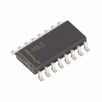
IC SWITCH QUAD SPST 16SOIC

DG441DY+

Manufacturer Part Number
DG441DY+
Description
IC SWITCH QUAD SPST 16SOIC
Manufacturer
Maxim Integrated Products
Type
Analog Switchr
Datasheet

Specifications of DG441DY+

Function
Switch
Circuit
4 x SPST - NC
On-state Resistance
85 Ohm
Voltage Supply Source
Single, Dual Supply
Voltage - Supply, Single/dual (±)
10 V ~ 30 V, ±4.5 V ~ 20 V
Operating Temperature
-40°C ~ 85°C
Mounting Type
Surface Mount
Package / Case
16-SOIC (0.154", 3.90mm Width)
Package
16SOIC N
Maximum On Resistance
160@10.8V Ohm
Maximum High Level Output Current
30 mA
Maximum Turn-off Time
200@12V ns
Maximum Turn-on Time
400@12V ns
Switch Architecture
SPST
Power Supply Type
Single|Dual
Lead Free Status / RoHS Status
Lead free / RoHS Compliant
Maxim’s redesigned DG441/DG442 analog switches
now feature on-resistance matching (4Ω max) between
switches and guaranteed on-resistance flatness over
the signal range (9Ω max). These low on-resistance
switches conduct equally well in either direction. They
guarantee low charge injection (10pC max), low power
consumption (1.65mW), and an ESD tolerance of 2000V
minimum per Method 3015.7. The new design offers
lower off-leakage current over temperature (less than
5nA at +85°C).
The DG441/DG442 are quad, single-pole/single-throw
(SPST) analog switches. The DG441 has four normally
closed switches, and the DG442 has four normally
open switches. Switching times are less than 250ns for
t
ate from a single +10V to +30V supply, or bipolar ±4.5V
to ±20V supplies. Maxim’s improved DG441/DG442
continue to be fabricated with a 44V silicon-gate
process.
Sample-and-Hold Circuits
Communication Systems
Test Equipment
Battery-Operated Systems
Heads-Up Displays
Fax Machines
19-4611; Rev 5; 5/09
For pricing, delivery, and ordering information, please contact Maxim Direct at 1-888-629-4642,
or visit Maxim’s website at www.maxim-ic.com.
ON
TOP VIEW
GND
IN1
IN4
D1
S1
S4
D4
V-
SWITCHES SHOWN FOR LOGIC “0” INPUT
and less than 170ns for t
1
2
3
4
5
6
7
8
LOGIC
1
0
DIP/SO
DG441
DG441
SWITCH
OFF
ON
_______________________________________________________________________________________
16
15
14
13
12
11
10
9
Improved, Quad, SPST Analog Switches
IN2
D2
S2
V+
N.C.
S3
D3
IN3
General Description
GND
IN1
IN4
D1
S1
S4
D4
V-
PBX, PABX
Guidance and Control
Systems
Audio-Signal Routing
Military Radios
Modems
OFF
1
2
3
4
5
6
7
8
N.C. = Not Internally Connected
Pin Configurations/Functional Diagrams/Truth Tables
LOGIC
. These devices oper-
0
1
DG442
DIP/SO
Applications
DG442
SWITCH
OFF
ON
16
15
14
13
12
11
10
9
IN2
S2
V+
N.C.
S3
D3
IN3
D2
TOP VIEW
GND
S1
S4
V-
*EP = EXPOSED PAD. CONNECT EXPOSED PAD TO V+.
1
2
3
4
D4
D1
16
*EP
5
♦ ♦ Plug-In Upgrades for Industry-Standard DG441/DG442
♦ ♦ Improved r DS(ON) Match Between Channels(4Ωmax)
♦ ♦ Guaranteed r FLAT(ON) Over Signal Range (9Ωmax)
♦ ♦ Improved Charge Injection (10pC max)
♦ ♦ Improved Off-Leakage Current Over Temperature
♦ ♦ Withstand Electrostatic Discharge (2000V min)
♦ ♦ Low r
♦ ♦ Single-Supply Operation +10V to +30V
♦ ♦ Low Power Consumption (1.65mW max)
♦ ♦ Rail-to-Rail Signal Handling
♦ ♦ TTL/CMOS-Logic Compatible
Ordering Information continued at end of data sheet.
Note: Devices are available in both leaded and lead(Pb)-free
packaging. Specify lead-free by adding the + symbol at the
end of the part number when ordering.
* Contact factory for dice specifications.
DG441CJ
DG441CY
DG441C/D
DG441DJ
DG441DY
THIN QFN
IN4
IN1
15
6
(<5nA at +85°C)
per Method 3015.7
Bipolar-Supply Operation ±4.5V to ±20V
DG441
PART
IN3
IN2
14
7
DS(ON)
D2
D3
13
8
(85Ω max)
12
11
10
9
S2
V+
N.C.
S3
-40°C to +85°C
-40°C to +85°C
TEMP RANGE
0°C to +70°C
0°C to +70°C
0°C to +70°C
GND
Ordering Information
S1
S4
V-
1
2
3
4
Existing Features
D4
D1
16
5
*EP
New Features
THIN QFN
IN4
IN1
15
6
DG442
PIN-PACKAGE
16 Plastic DIP
16 Narrow SO
Dice*
16 Plastic DIP
16 Narrow SO
IN3
IN2
14
7
D3
D2
13
8
12
11
10
9
S2
V+
N.C.
S3
1

Related parts for DG441DY+

DG441DY+ Summary of contents

Page 1

Rev 5; 5/09 Improved, Quad, SPST Analog Switches General Description Maxim’s redesigned DG441/DG442 analog switches now feature on-resistance matching (4Ω max) between switches and guaranteed on-resistance flatness over the signal range (9Ω max). These low on-resistance switches conduct equally ...

Page 2

Improved, Quad, SPST Analog Switches ABSOLUTE MAXIMUM RATINGS Voltage Referenced to V- V+.......................................................................................44V GND ...................................................................................25V V .................................................(GND - 0.3V) to (V+ + 0.3V) L Digital Inputs (Note 1)......(V- - 2V) to (V+ + 2V) or 30mA S ...

Page 3

Improved, Quad, SPST Analog Switches ELECTRICAL CHARACTERISTICS—Dual Supplies (continued) (V+ = 15V -15V 0V 2.4V, V GND INH PARAMETER SYMBOL SUPPLY Power-Supply Range V+, V- Positive Supply Current I+ Negative Supply Current I- Ground ...

Page 4

Improved, Quad, SPST Analog Switches ELECTRICAL CHARACTERISTICS—Single Supply (V+ = 12V 0V 0V 2.4V, V GND INH PARAMETER SYMBOL SWITCH Analog Signal Range V ANALOG Drain-Source r DS(ON) On-Resistance SUPPLY Power-Supply Range V+ Positive ...

Page 5

Improved, Quad, SPST Analog Switches ____________________________Typical Operating Characteristics (continued +25°C, unless otherwise noted.) A ON-RESISTANCE vs. V AND D UNIPOLAR SUPPLY VOLTAGE 250 225 200 175 150 125 V+ = 10V 100 V+ = 15V ...

Page 6

Improved, Quad, SPST Analog Switches Pin Description PIN NAME THIN DIP/SO QFN-EP 1, 16, 9, 15, 14, IN1–IN4 Input 15, 16, 13, D1–D4 Analog Switch Drain Terminal 10 14, 1, 12, 9, ...

Page 7

Improved, Quad, SPST Analog Switches ______________________________________________Timing Diagrams/Test Circuits LOGIC +3V INPUT 50 OFF V OUT 0 OUT SWITCH 0V OUTPUT t ON LOGIC INPUT WAVEFORM IS INVERTED FOR SWITCHES THAT HAVE THE OPPOSITE LOGIC SENSE. Figure ...

Page 8

Improved, Quad, SPST Analog Switches Timing Diagrams/ Test Circuits (continued) +15V 10nF +V D CAPACITANCE METER 1MHz GND Figure 6. Source/Drain-On/Off Capacitance For the latest package outline information and land patterns www.maxim-ic.com/packages. PACKAGE TYPE 16 ...

Page 9

... Maxim cannot assume responsibility for use of any circuitry other than circuitry entirely embodied in a Maxim product. No circuit patent licenses are implied. Maxim reserves the right to change the circuitry and specifications without notice at any time. Maxim Integrated Products, 120 San Gabriel Drive, Sunnyvale, CA 94086 408-737-7600 _____________________ 9 © 2009 Maxim Integrated Products DESCRIPTION Maxim is a registered trademark of Maxim Integrated Products, Inc ...

Related keywords