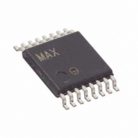
MAX4679EUE+ Maxim Integrated Products, MAX4679EUE+ Datasheet - Page 8

MAX4679EUE+
Manufacturer Part Number
MAX4679EUE+
Description
IC SWITCH QUAD SPST 16TSSOP
Manufacturer
Maxim Integrated Products
Datasheet
1.MAX4678EUE.pdf
(12 pages)
Specifications of MAX4679EUE+
Function
Switch
Circuit
4 x SPST - NC/NO
On-state Resistance
1.6 Ohm
Voltage Supply Source
Single, Dual Supply
Voltage - Supply, Single/dual (±)
2.7 V ~ 11 V, ±2.7 V ~ 5.5 V
Operating Temperature
-40°C ~ 85°C
Mounting Type
Surface Mount
Package / Case
16-TSSOP
Number Of Switches
Quad
Switch Configuration
SPST
On Resistance (max)
2 Ohms
On Time (max)
500 ns
Off Time (max)
350 ns
Off Isolation (typ)
- 65 dB
Bandwidth
66 MHz
Supply Voltage (max)
5.5 V
Supply Voltage (min)
2.7 V
Supply Current
1 uA
Maximum Power Dissipation
457 mW
Maximum Operating Temperature
+ 85 C
Mounting Style
SMD/SMT
Minimum Operating Temperature
- 40 C
Off State Leakage Current (max)
10 nA
Lead Free Status / RoHS Status
Lead free / RoHS Compliant
2Ω, Quad, SPST, CMOS Analog Switches
___________Applications Information
Proper power-supply sequencing is recommended for
all CMOS devices. Do not exceed the absolute maxi-
mum ratings because stresses beyond the listed ratings
can cause permanent damage to the devices. Always
sequence V+ on first, then V-, then V
logic inputs, NO_, NC_, or COM. If proper power-supply
sequencing is not possible, add two small signal diodes
(D1, D2) in series with the supply pins, and a Schottky
diode between V+ and V
(Figure 1). Adding diodes reduces the analog signal
range to one diode drop below V+ and one diode drop
above V-, but does not affect the devices’ low switch
resistance and low leakage characteristics. Device oper-
ation is unchanged, and the difference between V+ and
V- should not exceed 11V.
Figure 2. Switching Time
Figure 3. Break-Before-Make Interval (MAX4679 Only)
8
_______________________________________________________________________________________
LOGIC
INPUT
MAX4679
V
V
COM1
COM2
SWITCH
LOGIC
INPUT
INPUT
= +3V
= +3V
MAX4677
MAX4678
MAX4679
C
L
INCLUDES FIXTURE AND STRAY CAPACITANCE.
V
COM
COM1
COM2
I
I
N1
N2
GND
COM_
IN_
C
V
V+
V
OUT
L
L
INCLUDES FIXTURE AND STRAY CAPACITANCE.
GND
0V
= V
Overvoltage Protection
COM
L
V
V+
L
for overvoltage protection
(
V+
V+
V-
V-
R
L
R
+ R
NC2
L
NO1
OR NC_
ON
V+
V+
V-
V-
)
NO_
L
R
L2
followed by the
R
300Ω
L
R
C
V
C
L
L
OUT2
L2
= 300Ω
= 35pF
SWITCH
OUTPUT
C
35pF
R
L
L1
V
OUT
V
C
OUT1
L1
Power-supply bypassing improves noise margin and
prevents switching noise from propagating from the V+
supply to other components. A 0.1µF capacitor connect-
ed from V+ to GND is adequate for most applications.
Figure 1. Overvoltage Protection Using External Blocking Diodes
OUTPUT
SWITCH
LOGIC
INPUT
*INTERNAL PROTECTION DIODES
V
2
+3V
MAX4677
MAX4678
MAX4679
LOGIC
INPUT
SWITCH
OUTPUT 1
(V
SWITCH
OUTPUT 2
(V
0
0
OUT2
OUT1
COM_
)
)
+3V
V
0
0
0
OUT
t
ON
50%
*
*
0.9 x V
t D
50%
0UT
V+
V-
D1
D2
0.9 x V
t
OFF
0UT1
t r < 20ns
t f < 20ns
0.9 x V
*
*
t D
OUT
0.9 x V
V
NO_
L
OUT2


