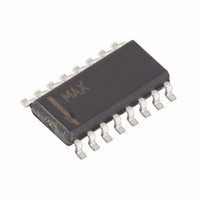
DG413DY+ Maxim Integrated Products, DG413DY+ Datasheet - Page 6

DG413DY+
Manufacturer Part Number
DG413DY+
Description
IC SWITCH QUAD SPST 16SOIC
Manufacturer
Maxim Integrated Products
Type
Analog Switchr
Datasheet
1.DG412CUE.pdf
(12 pages)
Specifications of DG413DY+
Function
Switch
Circuit
4 x SPST - NC/NO
On-state Resistance
45 Ohm
Voltage Supply Source
Single, Dual Supply
Voltage - Supply, Single/dual (±)
5 V ~ 44 V, ±5 V ~ 20 V
Operating Temperature
0°C ~ 70°C
Mounting Type
Surface Mount
Package / Case
16-SOIC (0.154", 3.90mm Width)
Number Of Switches
Quad
Switch Configuration
SPST
On Resistance (max)
45 Ohms
On Time (max)
175 ns
Off Time (max)
145 ns
Off Isolation (typ)
68 dB
Supply Voltage (max)
+/- 20 V
Supply Voltage (min)
+/- 4.5 V
Supply Current
0.0001 uA
Maximum Power Dissipation
696 mW
Maximum Operating Temperature
+ 85 C
Mounting Style
SMD/SMT
Description/function
Analog Switch
Input Level
CMOS, TTL
Minimum Operating Temperature
- 40 C
Off State Leakage Current (max)
5 nA
Package
16SOIC N
Maximum On Resistance
80@10.8V Ohm
Maximum High Level Output Current
30 mA
Maximum Turn-off Time
145@±15V ns
Maximum Turn-on Time
250@12V ns
Switch Architecture
SPST
Power Supply Type
Single|Dual
Lead Free Status / RoHS Status
Lead free / RoHS Compliant
Improved, Quad,
SPST Analog Switches
Using supply voltages other than 15V will reduce the
analog signal range. The DG411/DG412/DG413 switch-
es operate with ±4.5V to ±20V bipolar supplies or with
a +10V to +30V single supply; connect V- to 0V when
operating with a single supply. Also, all device types
can operate with unbalanced supplies such as +24V
and -5V. V
patible, or to V+ for CMOS-logic level inputs. The
Typical Operating Characteristics graphs show typical
on-resistance with ±15V, ±10V, and ±5V supplies.
(Switching times increase by a factor of two or more for
operation at ±5V.)
Proper power-supply sequencing is recommended for
all CMOS devices. Do not exceed the absolute maxi-
mum ratings because stresses beyond the listed rat-
ings may cause permanent damage to the devices.
Always sequence V+ on first, followed by V
logic inputs. If power-supply sequencing is not possi-
ble, add two small, external signal diodes in series with
supply pins for overvoltage protection (Figure 1).
6
__________Applications Information
DIP/SO/TSSOP
_______________________________________________________________________________________
2, 15, 10, 7
3, 14, 11, 6
1, 16, 9, 8
12
13
—
4
5
L
must be connected to +5V to be TTL com-
Operation with Supply Voltages
PIN
15, 14, 7, 6
16, 13, 8, 5
1, 12, 9, 4
Overvoltage Protection
QFN
10
11
—
2
3
Other Than 15V
IN1–IN4
D1–D4
NAME
S1–S4
GND
V+
V
EP
V-
L
L
, V-, and
Input
Analog Switch Drain Terminal
Analog Switch Source Terminal
Negative-Supply Voltage Input
Ground
Logic Supply Voltage
Positive-Supply Voltage Input—Connected to Substrate
Exposed Paddle (QFN Only). Connect EP to V+.
Adding diodes reduces the analog signal range to 1V
below V+ and 1V below V-, without affecting low switch
resistance and low leakage characteristics. Device
operation is unchanged, and the difference between
V+ and V- should not exceed +44V.
Figure 1. Overvoltage Protection Using External Blocking Diodes
V g
D
FUNCTION
V+
V-
V+
V-
Pin Description
S


