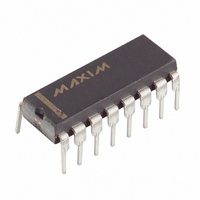
MAX308CPE+ Maxim Integrated Products, MAX308CPE+ Datasheet - Page 2

MAX308CPE+
Manufacturer Part Number
MAX308CPE+
Description
IC MULTIPLEXER 8X1 16DIP
Manufacturer
Maxim Integrated Products
Datasheet
1.MAX308CPE.pdf
(12 pages)
Specifications of MAX308CPE+
Function
Multiplexer
Circuit
1 x 8:1
On-state Resistance
100 Ohm
Voltage Supply Source
Single, Dual Supply
Voltage - Supply, Single/dual (±)
5 V ~ 30 V, ± 5 V ~ 20 V
Operating Temperature
0°C ~ 70°C
Mounting Type
Through Hole
Package / Case
16-DIP (0.300", 7.62mm)
Lead Free Status / RoHS Status
Lead free / RoHS Compliant
ABSOLUTE MAXIMUM RATINGS
Voltage Referenced to V-
Digital Inputs, NO, COM (Note 1)...........(V- - 2V) to (V+ + 2V) or
Continuous Current (any terminal) ......................................30mA
Peak Current, NO or COM
ELECTRICAL CHARACTERISTICS—Dual Supplies
(V+ = +15V, V- = -15V, GND = 0V, V
Precision, 8-Channel/Dual 4-Channel,
High-Performance, CMOS Analog Multiplexers
Note 1:
Stresses beyond those listed under “Absolute Maximum Ratings” may cause permanent damage to the device. These are stress ratings only, and functional
operation of the device at these or any other conditions beyond those indicated in the operational sections of the specifications is not implied. Exposure to
absolute maximum rating conditions for extended periods may affect device reliability.
2
SWITCH
Analog Signal Range
On-Resistance
On-Resistance Matching
Between Channels
On-Resistance Flatness
NO-Off Leakage Current
(Note 5)
COM-Off Leakage Current
(Note 5)
COM-On Leakage Current
(Note 5)
V+ ............................................................................-0.3V, 44V
GND .........................................................................-0.3V, 25V
(pulsed at 1ms, 10% duty cycle max) ..........................100mA
_______________________________________________________________________________________
PARAMETER
Signals on NO, COM, EN, A0, A1, or A2 exceeding V+ or V- are clamped by internal diodes. Limit forward current to
maximum current ratings.
I
SYMBOL
I
COM(OFF)
I
COM(ON)
30mA, (whichever occurs first)
NO(OFF)
R
V
∆R
V
R
COM
FLAT
NO
ON
AH
ON
,
= +2.4V, V
(Note 3)
I
V
I
V
I
V
V
V
V
V
V
V
V
V
V
V
V
sequence
each switch
on
NO
NO
NO
COM
COM
COM
COM
NO
EN
NO
COM
EN
NO
COM
EN
COM
NO
= -1.0mA,
= -1.0mA,
= -1.0mA,
= 0V
= 0V
= 0V
= ±10V,
= ±10V,
= +10V,
= ±10V,
AL
= ±10V
= ±10V (Note 4)
= ±5V or 0V
= +10V,
= +10V,
= ±10V,
= ±10V,
= +0.8V, T
MAX308
MAX309
MAX308
MAX309
CONDITIONS
A
= T
MIN
Continuous Power Dissipation (T
Operating Temperature Ranges
Storage Temperature Range .............................-65°C to +150°C
Lead Temperature (soldering, 10sec) .............................+300°C
T
T
T
T
T
T
T
T
to T
T
T
to T
T
T
to T
T
T
to T
T
T
to T
Plastic DIP (derate 10.53mW/°C above +70°C) ..........842mW
Narrow SO (derate 8.70mW/°C above +70°C) ............696mW
CERDIP (derate 10.00mW/°C above +70°C) ...............800mW
TSSOP (derate 6.7mW/°C above +70°C) ....................457mW
MAX30_C_ _ .......................................................0°C to +70°C
MAX30_E_ _.....................................................-40°C to +85°C
MAX30_MJE ..................................................-55°C to +125°C
A
A
A
A
A
A
A
A
A
A
A
A
A
A
A
A
to T
= +25°C
= T
= +25°C
= T
= +25°C
= T
= +25°C
= T
= +25°C
= T
= +25°C
= T
= +25°C
= T
= +25°C
= T
MAX
MAX
MAX
MAX
MAX
MAX
MIN
MIN
MIN
MIN
MIN
MIN
MIN
MIN
, unless otherwise noted.)
to T
to T
to T
C, E
M
C, E
M
C, E
M
C, E
M
C, E
M
MAX
MAX
MAX
-0.75
-0.75
-0.75
-0.75
MIN
-0.5
-2.5
-5.0
-15
-10
-20
-10
-10
-20
-10
-5
-5
A
= +70°C)
(Note 2)
TYP
0.01
0.02
0.02
0.02
0.02
1.5
1.8
60
MAX
0.75
0.75
0.75
0.75
100
125
0.5
2.5
5.0
15
10
10
20
10
10
20
10
5
8
7
5
5
UNITS
nA
nA
nA
Ω
Ω
Ω
V


