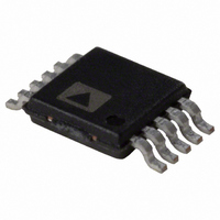
ADG787BRMZ Analog Devices Inc, ADG787BRMZ Datasheet

ADG787BRMZ
Specifications of ADG787BRMZ
Available stocks
Related parts for ADG787BRMZ
ADG787BRMZ Summary of contents
Page 1
FEATURES USB 1.1 signal switching compliant −3 dB bandwidth, 150 MHz Tiny 10-lead LFCSP and MSOP packages, 10-ball WLCSP package Single-supply 1 5.5 V operation Low on resistance 2.5 Ω typical 3.45 Ω maximum at 85°C Typical power ...
Page 2
ADG787 TABLE OF CONTENTS Features .............................................................................................. 1 Applications....................................................................................... 1 Functional Block Diagram .............................................................. 1 General Description ......................................................................... 1 Specifications..................................................................................... 3 Absolute Maximum Ratings............................................................ 5 ESD Caution.................................................................................. 5 REVISION HISTORY 5/06—Rev Rev. A Updated Formatting ...........................................................Universal Changes to Table ...
Page 3
SPECIFICATIONS 5.5 V, GND = 0 V, unless otherwise noted. DD Table 1. Parameter ANALOG SWITCH Analog Signal Range On Resistance ( Resistance Match Between Channels (ΔR On Resistance Flatness (R ) ...
Page 4
ADG787 3.6 V, GND = 0 V, unless otherwise noted. DD Table 2. Parameter ANALOG SWITCH Analog Signal Range On Resistance ( Resistance Match Between Channels (ΔR On Resistance Flatness (R ) ...
Page 5
ABSOLUTE MAXIMUM RATINGS T = 25°C, unless otherwise noted. A Table 3. Parameter Rating V to GND −0 Analog Inputs , Digital Inputs −0 Peak Current ...
Page 6
ADG787 PIN CONFIGURATIONS AND FUNCTION DESCRIPTIONS S1A 2 9 ADG787 TOP VIEW (Not to Scale) IN1 4 7 S1B 5 6 Figure 3. 10-Lead LFCSP and 10-lead MSOP Pin Configuration Table 4. 10-Lead ...
Page 7
TYPICAL PERFORMANCE CHARACTERISTICS 3 4. 4. 1.5 1.0 0 SIGNAL RANGE Figure 5. On Resistance vs 5.0 ...
Page 8
ADG787 2.0 1.5 1.0 0.5 0 –0.5 –1.0 –1.5 –2 TEMPERATURE (°C) Figure 11. Leakage Current vs. Temperature, V 2.0 1.8 1.6 1.4 1.2 V RISING V FALLING IN IN 1.0 0.8 0.6 0.4 ...
Page 9
V = 3V/4.2V/ 25°C A –20 –40 S1A TO S1B –60 –80 –100 –120 100 1k 10k 100k 1M 10M FREQUENCY (Hz) Figure 17. Crosstalk vs. Frequency 3V/4.2V/ 25°C A ...
Page 10
ADG787 1.2 INPUT RISE/FALL TIME = 15ns V = 4.2V DD 1.0 0.8 0.6 0.4 0.2 0 –40 – TEMPERATURE (°C) Figure 23. Rise-Time-to-Fall-Time Mismatch vs. Temperature 300 INPUT RISE/FALL TIME = 15ns T = 25°C A 250 ...
Page 11
TEST CIRCUITS V1 Figure 28. On Resistance V 0.1μF V S1B V S S1A IN GND V DD 0.1μ S1B V S S1A IN GND D V ...
Page 12
ADG787 V DD 0.1μ S1B S1A 50Ω GND V OUT OFF ISOLATION = 20 LOG VS Figure 34. Off Isolation 0.1μF S1A V OUT R L 50Ω S1B 50Ω CHANNEL-TO-CHANNEL CROSSTALK = 20 LOG ...
Page 13
TERMINOLOGY I DD Positive supply current Analog voltage on Terminal D and Terminal Ohmic resistance between D and S. R FLAT (ON) Flatness is defined as the difference between the maximum and ...
Page 14
ADG787 OUTLINE DIMENSIONS 1.50 BCS SQ 0.80 0.75 0.70 SEATING PLANE 3.10 3.00 2.90 PIN 1 0.95 0.85 0.75 0.15 0.05 INDEX AREA 3.00 BSC SQ 0.50 BSC TOP VIEW 0.50 0.40 0.80 MAX 0.30 0.55 TYP 0.05 MAX SIDE ...
Page 15
... IDENTIFIER TOP VIEW (BALL SIDE DOWN) ORDERING GUIDE Model Temperature Range ADG787BRMZ 2 –40°C to +85°C 2 ADG787BRMZ-500RL7 –40°C to +85°C ADG787BRMZ-REEL 2 –40°C to +85°C 2 ADG787BCBZ-500RL7 –25°C to +85°C 2 ADG787BCBZ-REEL –25°C to +85°C 2 ADG787BCPZ-500RL7 –40°C to +85°C ...
Page 16
ADG787 NOTES ©2006 Analog Devices, Inc. All rights reserved. Trademarks and registered trademarks are the property of their respective owners. D05250-0-5/06(A) Rev Page ...


