ADG413BNZ Analog Devices Inc, ADG413BNZ Datasheet - Page 4
ADG413BNZ
Manufacturer Part Number
ADG413BNZ
Description
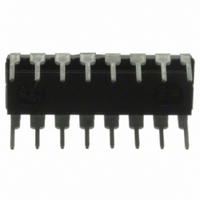
IC SWITCH QUAD SPST 16DIP
Manufacturer
Analog Devices Inc
Series
LC²MOSr
Specifications of ADG413BNZ
Operating Temperature
-40°C ~ 85°C
Function
Switch
Circuit
4 x SPST - NC/NO
On-state Resistance
35 Ohm
Voltage Supply Source
Single, Dual Supply
Voltage - Supply, Single/dual (±)
12V, ±15V
Current - Supply
1µA
Mounting Type
Through Hole
Package / Case
16-DIP (0.300", 7.62mm)
Analogue Switch Type
SPST
No. Of Channels
4
On State Resistance Max
35ohm
Turn Off Time
100ns
Turn On Time
110ns
Supply Voltage Range
10.8V To 13.2V, ± 13.5V To ± 16.5V
Lead Free Status / RoHS Status
Lead free / RoHS Compliant
Available stocks
Company
Part Number
Manufacturer
Quantity
Price
Company:

Part Number:
ADG413BNZ
Manufacturer:
ADI
Quantity:
14 565


ADG411/ADG412/ADG413
SINGLE SUPPLY
V
Table 2.
Parameter
ANALOG SIGNAL RANGE
LEAKAGE CURRENTS
DIGITAL INPUTS
DYNAMIC CHARACTERISTICS
POWER REQUIREMENTS
1
2
Table 3. Truth Table (ADG411/ADG412)
ADG411 In
0
1
Temperature ranges are as follows: B versions:−40°C to +85°C; T versions: −55°C to +125°C.
Guaranteed by design; not subject to production test.
DD
R
Source OFF Leakage I
Drain OFF Leakage I
Channel ON Leakage I
Input High Voltage, V
Input Low Voltage, V
Input Current
I
t
t
Break-Before-Make Time
Delay, t
Charge Injection
OFF Isolation
Channel-to-Channel Crosstalk
C
C
C
I
I
INL
DD
L
ON
OFF
ON
S
D
D
= 12 V ± 10%, V
, C
(OFF)
(OFF)
or I
S
(ON)
INH
D
(ADG413 Only)
ADG412 In
1
0
SS
D
INL
= 0 V, V
INH
S
(OFF)
D
, I
(OFF)
S
(ON)
2
L
= 5 V ± 10%, GND = 0 V, unless otherwise noted.
+25°C
40
80
±0.1
±0.25
±0.1
±0.25
±0.1
±0.4
0.005
175
95
25
25
68
85
9
9
35
0.0001
1
0.0001
1
Switch Condition
ON
OFF
B Version
−40°C to + 85°C
0 V to V
100
±5
±5
±10
2.4
0.8
±0.5
250
125
5
5
DD
Rev. D | Page 4 of 16
+25°C
40
80
±0.1
±0.25
±0.1
±0.25
±0.1
±0.4
0.005
175
95
25
25
68
85
9
9
35
0.0001
1
0.0001
1
Table 4. Truth Table (ADG413)
Logic
0
1
T Version
−55°C to +125°C
0 V to V
100
±20
±20
±40
2.4
0.8
±0.5
250
125
5
5
1
DD
Switch 1, 4
OFF
ON
Unit
V
Ω typ
Ω max
nA typ
nA max
nA typ
nA max
nA typ
nA max
V min
V max
μA typ
μA max
ns typ
ns max
ns typ
ns max
ns typ
pC typ
dB typ
dB typ
pF typ
pF typ
pF typ
μA typ
μA max
μA typ
μA max
Test Conditions/Comments
0 < V
V
V
V
Figure 15
V
Figure 15
V
Figure 16
V
R
V
R
V
R
V
V
Figure 19
R
Figure 20
R
Figure 21
f = 1 MHz
f = 1 MHz
f = 1 MHz
V
Digital inputs = 0 V or 5 V
V
L
L
L
L
L
DD
DD
D
D
D
IN
S
S
S1
S
DD
L
= 300 Ω, C
= 8 V; Figure 17
= 300 Ω, C
= 8 V; Figure 17
= 300 Ω, C
= 0 V, R
= 50 Ω, C
= 50 Ω, C
= 5.25 V
= 12.2 V/1 V, V
= 12.2 V/1 V, V
= V
= V
= V
= 10.8 V
= 13.2 V
= 13.2 V;
D
INL
S
S2
= 8.5 V, I
= 12.2 V/1 V;
= +10 V; Figure 18
Switch 2, 3
ON
OFF
or V
S
= 0 Ω, C
L
L
= 5 pF, f = 1 MHz;
= 5 pF, f = 1 MHz;
INH
L
L
L
= 35 pF;
= 35 pF;
= 35 pF;
S
= −10 mA;
S
S
= 1 V/12.2 V;
= 1 V/12.2 V;
L
= 10 nF;
Related parts for ADG413BNZ
Image
Part Number
Description
Manufacturer
Datasheet
Request
R

Part Number:
Description:
±1.7g Dual-Axis IMEMS Accelerometer Evaluation Board
Manufacturer:
Analog Devices Inc
Datasheet:

Part Number:
Description:
Inertial Sensor Evaluation System
Manufacturer:
Analog Devices Inc
Datasheet:
Part Number:
Description:
Manufacturer:
Analog Devices Inc
Datasheet:
Part Number:
Description:
Manufacturer:
Analog Devices Inc
Datasheet:
Part Number:
Description:
Manufacturer:
Analog Devices Inc
Datasheet:
Part Number:
Description:
Manufacturer:
Analog Devices Inc
Datasheet:
Part Number:
Description:
Manufacturer:
Analog Devices Inc
Datasheet:
Part Number:
Description:
Manufacturer:
Analog Devices Inc
Datasheet:
Part Number:
Description:
Manufacturer:
Analog Devices Inc
Datasheet:
Part Number:
Description:
Manufacturer:
Analog Devices Inc
Datasheet:
Part Number:
Description:
Manufacturer:
Analog Devices Inc
Datasheet:
Part Number:
Description:
Manufacturer:
Analog Devices Inc
Datasheet:
Part Number:
Description:
Manufacturer:
Analog Devices Inc
Datasheet: