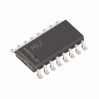
MAX4709ESE+ Maxim Integrated Products, MAX4709ESE+ Datasheet - Page 11

MAX4709ESE+
Manufacturer Part Number
MAX4709ESE+
Description
IC MULTIPLEXER DUAL 4X1 16SOIC
Manufacturer
Maxim Integrated Products
Type
Analog Multiplexerr
Datasheet
1.MAX4709ESE.pdf
(15 pages)
Specifications of MAX4709ESE+
Function
Multiplexer
Circuit
2 x 4:1
On-state Resistance
400 Ohm
Voltage Supply Source
Single, Dual Supply
Voltage - Supply, Single/dual (±)
9 V ~ 36 V, ±4.5 V ~ 20 V
Operating Temperature
-40°C ~ 85°C
Mounting Type
Surface Mount
Package / Case
16-SOIC (0.154", 3.90mm Width)
Number Of Channels
2 Channel
On Resistance (max)
950 Ohms at 12 V
Propagation Delay Time
350 ns at +/- 15 V, 400 ns at 12 V
On Time (max)
500 ns at 12 V
Off Time (max)
250 ns at 12 V
Supply Voltage (max)
36 V
Supply Voltage (min)
9 V
Maximum Power Dissipation
696 mW
Maximum Operating Temperature
+ 85 C
Minimum Operating Temperature
- 40 C
Mounting Style
SMD/SMT
Switch Current (typ)
0.37 mA at 15 V, - 0.2 mA at - 15 V
Lead Free Status / RoHS Status
Lead free / RoHS Compliant
V+ and GND power the internal logic and logic-level trans-
lators. The logic-level translators convert the logic-level
inputs to V+ and V- to drive the gates of the internal FETs.
In this design, there is no galvanic connection inside the
MAX4708/MAX4709 between the analog signal paths and
GND. ESD-protection diodes connect A_ to V+ and V-.
Driving the logic signals rail-to-rail from 0 to +15V or
-15V to +15V reduces the current consumption from
370µA (typ) to 200µA (typ) (see the Electrical Charac-
teristic s table, Power Supplies).
The MAX4708/MAX4709 operate with bipolar supplies
between ±4.5V and ±20V. The V+ and V- supplies
need not be symmetrical, but V+ - V- cannot exceed
the 44V absolute maximum rating.
The MAX4708/MAX4709 operate from single supplies
between +9V and +36V when V- is connected to GND.
Figure 1. Functional Diagram
NO_
GND
A_
V+
V-
Applications Information
______________________________________________________________________________________
ESD DIODES
Supply Current Reduction
Pin Configurations/Functional Diagrams (continued)
Power Supplies
NORMALLY OPEN SWITCH CONSTRUCTION
Fault-Protected, Single 8-to-1/
FAULT
FAULT
HIGH
LOW
Ground
ON
Dual 4-to-1 Multiplexers
PROCESS: CMOS
SUBSTRATE INTERNALLY CONNECTED TO V+
For the latest package outline information and land patterns, go
to www.maxim-ic.com/packages.
PACKAGE TYPE
16 Narrow SO
16 Plastic DIP
16 Wide SO
N1
PACKAGE CODE
Package Information
P1
MAX4708
MAX4709
—
—
—
Chip Information
DOCUMENT NO.
COM_
21-0041
21-0042
21-0043
11


