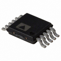
ADG836YRM-REEL7 Analog Devices Inc, ADG836YRM-REEL7 Datasheet

ADG836YRM-REEL7
Specifications of ADG836YRM-REEL7
Available stocks
Related parts for ADG836YRM-REEL7
ADG836YRM-REEL7 Summary of contents
Page 1
FEATURES 0.5 Ω typical on resistance 0.8 Ω maximum on resistance at 125°C 1. 3.6 V operation Automotive temperature range: –40°C to +125°C High current carrying capability: 300 mA continuous Rail-to-rail switching operation Fast-switching times <20 ns Typical ...
Page 2
ADG836 TABLE OF CONTENTS Specifications..................................................................................... 3 Absolute Maximum Ratings............................................................ 6 ESD Caution.................................................................................. 6 Pin Configurations ........................................................................... 7 REVISION HISTORY 4/05—Rev Rev. A Updated Format..................................................................Universal Changes to Table 1............................................................................ 3 Changes to Table 2............................................................................ 4 Changes to Table 3............................................................................ ...
Page 3
SPECIFICATIONS 3.6 V, GND = 0 V, unless otherwise noted. DD Table 1. Parameter ANALOG SWITCH Analog Signal Range On Resistance ( Resistance Match Between Channels (∆ Resistance Flatness ...
Page 4
ADG836 V = 2.5 V ± 0.2 V, GND = 0 V, unless otherwise noted. DD Table 2. Parameter ANALOG SWITCH Analog Signal Range On Resistance ( Resistance Match Between Channels (∆ Resistance Flatness ...
Page 5
V = 1.65 V ± 1.95 V, GND = 0 V, unless otherwise noted. DD Table 3. Parameter ANALOG SWITCH Analog Signal Range On Resistance ( Resistance Match Between Channels (∆ LEAKAGE CURRENTS Source Off ...
Page 6
ADG836 ABSOLUTE MAXIMUM RATINGS T = 25°C, unless otherwise noted. A Table 4. Parameter V to GND DD 1 Analog Inputs 1 Digital Inputs Peak Current 3.3 V Operation 2.5 V Operation 1.8 V Operation Continuous Current, ...
Page 7
PIN CONFIGURATIONS IN1 1 10 S1A 2 9 ADG836 GND 3 8 TOP VIEW (Not to Scale) S2A 4 7 IN2 5 6 Figure 2. 10-Lead MSOP (RM-10) Table 6. Terminology V Most positive power supply potential Positive ...
Page 8
ADG836 TYPICAL PERFORMANCE CHARACTERISTICS 0. 25° 0.50 0.45 0. 3.6V DD 0.35 0.30 0.25 0.20 0 0.5 1.0 1 Figure 4. On Resistance ...
Page 9
–20 I –40 –60 – TEMPERATURE (°C) Figure 10. Leakage Current vs. Temperature ...
Page 10
ADG836 0 – 25° 3.3V/2.5V/1.8V CC –20 –30 –40 –50 –60 –70 –80 0.01 0 FREQUENCY (MHz) Figure 16. Off Isolation vs. Frequency –10 S1A–S1B – 25°C A – ...
Page 11
TEST CIRCUITS V1 Figure 19. On Resistance V 0.1µF V S1B V S S1A IN GND V DD 0.1µ S1B V S S1A IN GND D V ...
Page 12
ADG836 V DD 0.1µ S1B S1A 50Ω GND V OUT OFF ISOLATION = 20 LOG VS Figure 25. Off Isolation V DD 0.1µ S1B S1A D GND V WITH SWITCH OUT INSERTION LOSS = ...
Page 13
... SEATING PLANE ORDERING GUIDE Model Temperature Range ADG836YRM –40°C to +125°C ADG836YRM-REEL –40°C to +125°C ADG836YRM-REEL7 –40°C to +125°C ADG836YRMZ 2 –40°C to +125°C 2 ADG836YRMZ-REEL –40°C to +125°C ADG836YRMZ-REEL7 2 –40°C to +125°C ADG836YCP-REEL – ...
Page 14
ADG836 NOTES Rev Page ...
Page 15
NOTES Rev Page ADG836 ...
Page 16
ADG836 NOTES © 2005 Analog Devices, Inc. All rights reserved. Trademarks and registered trademarks are the property of their respective owners. C04308-0-4/05(A) Rev Page ...


