HI1-0303-5 Intersil, HI1-0303-5 Datasheet
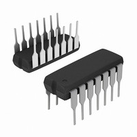
IC SWITCH DUAL SPDT 14CDIP

HI1-0303-5

Manufacturer Part Number
HI1-0303-5
Description
IC SWITCH DUAL SPDT 14CDIP
Manufacturer
Intersil
Datasheet

Specifications of HI1-0303-5

Function
Switch
Circuit
2 x SPDT
On-state Resistance
50 Ohm
Voltage Supply Source
Single, Dual Supply
Voltage - Supply, Single/dual (±)
5 V ~ 34 V, ±5 V ~ 20 V
Operating Temperature
0°C ~ 75°C
Mounting Type
Through Hole
Package / Case
14-CDIP (0.300", 7.62mm)
Lead Free Status / RoHS Status
Contains lead / RoHS non-compliant
Dual, SPDT CMOS Analog Switch
The HI-303 switch is a monolithic device fabricated using
CMOS technology and the Intersil dielectric isolation
process. This switch features break-before-make switching,
low and nearly constant ON resistance over the full analog
signal range, and low power dissipation.
The HI-303 is TTL compatible and has a logic “0” condition
with an input less than 0.8V and a logic “1” condition with an
input greater than 4V. (See pinouts for switch conditions with
a logic “1” input.)
Functional Diagram
Pinout
IN
Switch States Shown For A Logic “1” Input
LOGIC
HI-303 (PDIP, CERDIP, SOIC)
0
1
GND
IN
NC
D
D
S
S
3
3
1
1
1
7
1
2
3
4
5
6
SW1, SW2
TOP VIEW
®
OFF
ON
N
1
Data Sheet
14
13
12
10
11
SW3, SW4
9
8
V+
S
D
D
S
IN
V-
OFF
ON
P
4
2
4
2
2
S
D
1-888-INTERSIL or 321-724-7143
CAUTION: These devices are sensitive to electrostatic discharge; follow proper IC Handling Procedures.
Features
• Analog Signal Range (±15V Supplies) . . . . . . . . . . ±15V
• Low Leakage at 25
• Low Leakage at 125
• Low On Resistance at 25
• Break-Before-Make Delay . . . . . . . . . . . . . . . . . . . . 60ns
• Charge Injection . . . . . . . . . . . . . . . . . . . . . . . . . . . 30pC
• TTL, CMOS Compatible
• Symmetrical Switch Elements
• Low Operating Power (Typ) . . . . . . . . . . . . . . . . . . . . 1.0mW
• Pb-Free Available (RoHS Compliant)
Applications
• Sample and Hold (i.e., Low Leakage Switching)
• Op Amp Gain Switching (i.e., Low On Resistance)
• Portable, Battery Operated Circuits
• Low Level Switching Circuits
• Dual or Single Supply Systems
Ordering Information
NOTE: Intersil Pb-free products employ special Pb-free material sets;
molding compounds/die attach materials and 100% matte tin plate
termination finish, which are RoHS compliant and compatible with
both SnPb and Pb-free soldering operations. Intersil Pb-free products
are MSL classified at Pb-free peak reflow temperatures that meet or
exceed the Pb-free requirements of IPC/JEDEC J STD-020C.
HI1-0303-2
HI1-0303-5
HI3-0303-5
HI3-0303-5Z
(See Note)
HI9P0303-9
HI9P0303-9Z
(See Note)
November 17, 2004
NUMBER
PART
All other trademarks mentioned are the property of their respective owners.
|
Intersil (and design) is a registered trademark of Intersil Americas Inc.
Copyright © Intersil Americas Inc. 2003, 2004. All Rights Reserved
RANGE (
-55 to 125
-40 to 85
-40 to 85
TEMP.
0 to 75
0 to 75
0 to 75
o
C . . . . . . . . . . . . . . . . . . . . . . . 40pA
o
C . . . . . . . . . . . . . . . . . . . . . . . 1nA
o
C)
o
C . . . . . . . . . . . . . . . . . . . 35Ω
14 Ld CERDIP
14 Ld CERDIP
14 Ld PDIP
14 Ld PDIP
(Pb-free)
14 Ld SOIC
14 Ld SOIC
(Pb-free)
PACKAGE
FN3125.10
HI-303
F14.3
F14.3
E14.3
E14.3
M14.15
M14.15
PKG. DWG.
#

Related parts for HI1-0303-5

HI1-0303-5 Summary of contents

Page 1

... D 2 PART S 2 NUMBER IN 2 HI1-0303-2 V- HI1-0303-5 HI3-0303-5 HI3-0303-5Z (See Note) ON HI9P0303-9 OFF HI9P0303-9Z (See Note) NOTE: Intersil Pb-free products employ special Pb-free material sets; molding compounds/die attach materials and 100% matte tin plate termination finish, which are RoHS compliant and compatible with both SnPb and Pb-free soldering operations ...

Page 2

Schematic Diagrams D2A MP1A 200Ω LOGIC IN D1A MN1A GND V- 2 HI-303 V+ MN1B MN2B MN3B MP5B MP4B MN4B MP3B MP2B MP1B SWITCH CELL MP2A MP3A MP4A MN2A MN3A MN4A DIGITAL INPUT BUFFER AND LEVEL ...

Page 3

Absolute Maximum Ratings Voltage Between Supplies ( 44V (±22V) Digital Input Voltage . . . . . . . . . . ...

Page 4

Electrical Specifications Supplies = +15V, -15V; V Unless Otherwise Specified (Continued) PARAMETER POWER SUPPLY CHARACTERISTICS Current, I+ (Note 8) Current, I- (Note 8) Current, I+ (Note 9) Current, I- (Note 9) NOTES: = ±10V 10mA. On ...

Page 5

Test Circuits and Waveforms +15V GEN S V GEN IN V- GND V LOGIC -15V FIGURE 2A. TEST CIRCUIT 10V GEN 0 0 0.4 0.8 TIME (µs) FIGURE 2C. V ANALOG 5 ...

Page 6

Test Circuits and Waveforms NOTE: 11 increased, there will be proportional increases in rise and/or fall RC times. GEN L L FIGURE 2. SWITCHING WAVEFORMS FOR VARIOUS ANALOG INPUT VOLTAGES 15V V+ S ...

Page 7

Typical Performance Curves 100 V+ = +15V -15V 15V 1.0 0 100 1K LOGIC SWITCHING FREQUENCY (50% DUTY CYCLE) (Hz) FIGURE 6. ...

Page 8

Typical Performance Curves 300 V+ = +15V -15V V = 4.0V INH INL t ON 200 t OFF 100 -55 -35 - TEMPERATURE ( FIGURE 12. SWITCHING TIME vs TEMPERATURE 1.8 1.6 ...

Page 9

Dual-In-Line Plastic Packages (PDIP INDEX N/2 AREA -B- -A- D BASE PLANE -C- SEATING PLANE 0.010 (0.25 NOTES: 1. Controlling Dimensions: INCH. In case of conflict between ...

Page 10

Ceramic Dual-In-Line Frit Seal Packages (CERDIP) -D- -A- E -B- bbb BASE Q PLANE -C- SEATING PLANE aaa ccc ...

Page 11

... Accordingly, the reader is cautioned to verify that data sheets are current before placing orders. Information furnished by Intersil is believed to be accurate and reliable. However, no responsibility is assumed by Intersil or its subsidiaries for its use; nor for any infringements of patents or other rights of third parties which may result from its use ...

Related keywords