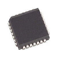
CY7B923-400JC Cypress Semiconductor Corp, CY7B923-400JC Datasheet - Page 9

CY7B923-400JC
Manufacturer Part Number
CY7B923-400JC
Description
Manufacturer
Cypress Semiconductor Corp
Datasheet
1.CY7B923-400JC.pdf
(33 pages)
Specifications of CY7B923-400JC
Lead Free Status / Rohs Status
Not Compliant
Available stocks
Company
Part Number
Manufacturer
Quantity
Price
Company:
Part Number:
CY7B923-400JC
Manufacturer:
CYPRESS
Quantity:
210
Document #: 38-02017 Rev. *E
Bypass Mode Operation
In Bypass mode the input data is interpreted as ten (10) bits
(D
data to be serialized and sent over the link. This data can use
any encoding method suitable to the designer. The only
restrictions upon the data encoding method is that it contain
suitable transition density for the Receiver PLL data synchro-
nizer (one per 10 bit byte), and that it be compatible with the
transmission media.
Data loaded into the Input register on the rising edge of CKW
will be loaded into the Shifter on the subsequent rising edges
of CKW. It will then be shifted to the outputs one bit at a time
using the internal clock generated by the clock generator. The
first bit of the transmission character (D
output (OUTA±, OUTB±, and OUTC±) after the next CKW
edge.
While in either the Encoded mode or Bypass mode, if a CKW
edge arrives when the inputs are not enabled (ENA and ENN
both HIGH), the Encoder will insert a pad character K28.5
(e.g., C5.0) to maintain proper link synchronization (in Bypass
b–h
), SC/D (D
a
), and SVS (D
ENA
CKR
HOTLink TRANSMITTER
ASYNCHRONOUS FIFO
ASYNCHRONOUS FIFO
CKW
HOTLink RECEIVER
RDY
7C42X/3X/6X/7X
7C42X/3X/6X/7X
W
j
) of pre-encoded transmission
7B923
7B933
RP
R
a
) will appear at the
Q
D
Figure 4. Seamless FIFO Interface
0–7
0–7
Q
D
0–8
, SC/D
, SC/D
0–8
9
9
mode the proper sense of running disparity cannot be
guaranteed for the first pad character, but is correct for all pad
characters that follow). This automatic insertion of pad
characters can be inhibited by insuring that the Transmitter is
always enabled (i.e., ENA or ENN is hard-wired LOW).
PECL Output Functional and Connection Options
The three pairs of PECL outputs all contain the same infor-
mation and are intended for use in systems with multiple
connections. Each output pair may be connected to a different
serial media, each of which may be a different length, link type,
or interface technology. For systems that do not require all
three output pairs, the unused pairs should be wired to V
minimize the power dissipated by the output circuit, and to
minimize unwanted noise generation. An internal voltage
comparator detects when an output differential pair is wired to
V
This results in a power savings of around 5 mA for each
unused pair.
In systems that require the outputs to be shut off during some
periods when link transmission is prohibited (e.g., for laser
CC
, causing the current source for that pair to be disabled.
ENN
ENR
CKR
CKW
HOTLink TRANSMITTER
HOTLink RECEIVER
CKW
CKR
CLOCKED FIFO
CLOCKED FIFO
ENW
RDY
7C44X/5X
7C44X/5X
7B923
7B933
D
Q
0–7
0–7
Q
D
0–8
, SC/D
0–8
, SC/D
9
9
CY7B923
CY7B933
Page 9 of 33
CC
to


