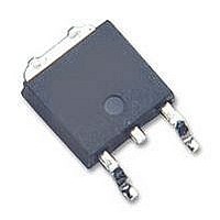
AUIRFR9024N International Rectifier, AUIRFR9024N Datasheet - Page 2

AUIRFR9024N
Manufacturer Part Number
AUIRFR9024N
Description
54T8918
Manufacturer
International Rectifier
Datasheet
1.AUIRFR9024N.pdf
(13 pages)
Specifications of AUIRFR9024N
Transistor Polarity
P Channel
Continuous Drain Current Id
-11A
Drain Source Voltage Vds
-55V
On Resistance Rds(on)
0.175ohm
Rds(on) Test Voltage Vgs
-10V
Power Dissipation Pd
38W
Rohs Compliant
Yes
Configuration
Single
Resistance Drain-source Rds (on)
175 mOhms
Drain-source Breakdown Voltage
55 V
Gate-source Breakdown Voltage
+/- 20 V
Continuous Drain Current
11 A
Power Dissipation
38 W
Mounting Style
SMD/SMT
Package / Case
DPAK
Gate Charge Qg
12.7 nC
Minimum Operating Temperature
- 55 C
Lead Free Status / Rohs Status
Details
Available stocks
Company
Part Number
Manufacturer
Quantity
Price
Company:
Part Number:
AUIRFR9024N
Manufacturer:
IR
Quantity:
12 500
Notes:
V
∆V
R
V
gfs
I
I
Q
Q
Q
t
t
t
t
L
L
C
C
C
I
I
V
t
Q
t
‚
ƒ
Static Electrical Characteristics @ T
Dynamic Electrical Characteristics @ T
Diode Characteristics
** When mounted on 1" square PCB (FR-4 or G-10 Material).
DSS
GSS
d(on)
r
d(off)
f
S
SM
rr
on
D
S
(BR)DSS
DS(on)
GS(th)
iss
oss
rss
SD
g
gs
gd
rr
Repetitive rating; pulse width limited by
max. junction temperature. (See fig. 11).
Starting T
R
I
T
For recommended footprint and soldering techniques refer to application note #AN-994.
(BR)DSS
2
SD
J
G
≤ 150 C
= 25Ω, I
≤ -6.6A, di/dt ≤ -240A/ s, V
/∆T
J
J
= 25°C, L = 2.8mH
AS
= -6.6A (See Figure 12)
Drain-to-Source Breakdown Voltage
Breakdown Voltage Temp. Coefficient
Static Drain-to-Source On-Resistance
Gate Threshold Voltage
Forward Transconductance
Drain-to-Source Leakage Current
Gate-to-Source Forward Leakage
Gate-to-Source Reverse Leakage
Total Gate Charge
Gate-to-Source Charge
Gate-to-Drain ("Miller") Charge
Turn-On Delay Time
Rise Time
Turn-Off Delay Time
Fall Time
Internal Drain Inductance
Internal Source Inductance
Input Capacitance
Output Capacitance
Reverse Transfer Capacitance
Continuous Source Current
(Body Diode)
Pulsed Source Current
(Body Diode)
Diode Forward Voltage
Reverse Recovery Time
Reverse Recovery Charge
Forward Turn-On Time
Parameter
DD
Parameter
™
≤ V
(BR)DSS
,
J
= 25°C (unless otherwise specified)
J
= 25°C (unless otherwise specified)
Intrinsic turn-on time is negligible (turn-on is dominated by LS+LD)
Min.
Min.
–––
–––
–––
–––
–––
–––
–––
–––
–––
–––
–––
–––
–––
–––
–––
–––
–––
–––
–––
–––
–––
–––
–––
-2.0
2.5
-55
„
… This is applied for I-PAK, L
† Uses IRF9Z24N data and test conditions.
Pulse width ≤ 300 s; duty cycle ≤ 2%.
lead and center of die contact.
Typ.
-0.05
Typ.
–––
–––
–––
–––
–––
–––
–––
–––
–––
–––
–––
–––
350
170
–––
–––
4.5
7.5
13
55
23
37
92
47
84
Max. Units
0.175
Max. Units
-100
–––
–––
–––
-250
100
–––
–––
–––
–––
–––
–––
–––
–––
–––
-1.6
130
-4.0
-11
-44
5.1
-25
19
10
71
V/°C
µA
nA
nC
nH
nC
ns
pF
ns
Ω
V
V
S
A
V
V
Reference to 25°C, I
V
V
V
V
V
V
V
I
V
V
V
I
R
R
Between lead,
6mm (0.25in.)
from package
and center of die contact
V
V
ƒ = 1.0MHz,see Fig.5
MOSFET symbol
showing the
integral reverse
p-n junction diode.
T
T
di/dt = 100A/µs
D
D
J
J
GS
GS
DS
DS
DS
DS
GS
GS
DS
GS
DD
G
D
GS
DS
= -7.2A
= -7.2A
S
= 25°C, I
= 25°C, I
= 3.7Ω, See Fig.10
= 24 Ω
= 0V, I
= -10V, I
= V
= -25V, I
= -55V, V
= -44V, V
= -20V
= 20V
= -44V
= -10V,See Fig 6 and 13
= -28V
= 0V
= -25V
of D-PAK is measured between
GS
, I
D
D
S
F
= -250µA
D
D
= -250µA
GS
GS
= -7.2A, V
= -7.2A
= -7.2A
= -6.6A
fh
Conditions
Conditions
= 0V
= 0V, T
D
= -1mA
h
f
h
J
GS
fh
= 150°C
= 0V
www.irf.com
fh
G
G
f
S
D
D
S


