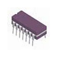
DS1488J National Semiconductor, DS1488J Datasheet - Page 2

DS1488J
Manufacturer Part Number
DS1488J
Description
Manufacturer
National Semiconductor
Datasheet
1.DS1488J.pdf
(8 pages)
Specifications of DS1488J
Number Of Receivers
Not Required
Number Of Transmitters
4
Number Of Transceivers
Not Required
Data Transmission Topology
Point-to-Point
Receiver Signal Type
Not Required
Transmitter Signal Type
Single-Ended
Single Supply Voltage (typ)
Not RequiredV
Single Supply Voltage (min)
Not RequiredV
Single Supply Voltage (max)
Not RequiredV
Dual Supply Voltage (max)
±15V
Supply Current
34mA
Power Supply Requirement
Dual
Operating Temp Range
0C to 75C
Operating Temperature Classification
Commercial
Mounting
Through Hole
Pin Count
14
Package Type
CDIP
Lead Free Status / Rohs Status
Not Compliant
Available stocks
Company
Part Number
Manufacturer
Quantity
Price
Part Number:
DS1488J
Manufacturer:
NS/国半
Quantity:
20 000
www.national.com
I
I
V
V
I
I
R
I
I
P
t
t
t
t
IL
IH
OS
OS
CC
CC
pd1
pd0
r
f
Symbol
Symbol
OH
OL
d
OUT
Absolute Maximum Ratings
If Military/Aerospace specified devices are required,
please contact the National Semiconductor Sales Office/
Distributors for availability and specifications.
Electrical Characteristics
V
Switching Characteristics
(V
Note 2: “Absolute Maximum Ratings” are those values beyond which the safety of the device cannot be guaranteed. Except for “Operating Temperature Range”
they are not meant to imply that the devices should be operated at these limits. The table of “Electrical Characteristics” provides conditions for actual device
operation.
Note 3: Unless otherwise specified min/max limits apply across the 0°C to +75°C temperature range for the DS1488.
+
−
+
−
CC
CC
+ = 9V, V
Supply Voltage
Input Voltage (V
Output Voltage
= 9V, V
V
V
+
−
Logical “0” Input Current
Logical “1” Input Current
High Level Output Voltage
Low Level Output Voltage
High Level Output
Short-Circuit Current
Low Level Output
Short-Circuit Current
Output Resistance
Positive Supply Current
(Output Open)
Negative Supply Current
(Output Open)
Power Dissipation
Propagation Delay to a Logical “1”
Propagation Delay to a Logical “0”
Rise Time
Fall Time
EE
CC
= −9V, T
− = −9V unless otherwise specified
Parameter
IN
)
A
= 25°C)
Parameter
5776 Version 8 Revision 5
−15V
V
V
R
V
R
V
V
V
V
V
V
V
V
V
V
IN
IN
L
IN
L
IN
OUT
OUT
+
IN
IN
IN
IN
+
+
(Note
= 3.0 kΩ,
= 3.0 kΩ,
= V
= 9.0V, V
= 12V, V
= 0V
= +5.0V
= 0.8V
= 1.9V
= 1.9V
= 0.8V
= 1.9V
= 0.8V
(Note
≤
= 0V, V
= 0V, V
−
+15V
−15V
V
±15V
= 0V, V
7.0V
3,
IN
Note
2)
≤
−
−
R
R
R
R
IN
IN
= −12V
= −9.0V
L
L
L
L
= 0.8V
= 1.9V
OUT
= 3.0 kΩ, C
= 3.0 kΩ, C
= 3.0 kΩ, C
= 3.0 kΩ, C
4)
Conditions
V
V
V
V
V
V
V
V
V
V
V
V
V
V
V
V
Print Date/Time: 2010/07/13 23:56:21
+
+
+
+
= ±2V
+
+
+
+
+
+
+
+
+
+
+
+
= 9.0V, V
= 13.2V, V
= 9.0V, V
= 13.2V, V
= 9.0V, V
= 12V, V
= 15V, V
= 9.0V, V
= 12V, V
= 15V, V
= 9.0V, V
= 12V, V
= 15V, V
= 9.0V, V
= 12V, V
= 15V, V
2
Note 1: Derate molded DIP package 10.2 mW/°C above 25°C; derate SO
package 7.8 mW/°C above 25°C.
L
L
L
L
Conditions
= 15 pF, T
= 15 pF, T
= 15 pF, T
= 15 pF, T
−
−
−
−
−
−
−
−
−
−
−
−
−
−
Operating Temperature Range
Storage Temperature Range
Maximum Power Dissipation
Lead Temperature (Soldering, 4
sec.)
= −12V
= −15V
= −12V
= −15V
= −12V
= −15V
= −12V
= −15V
−
−
= −9.0V
= −9.0V
= −9.0V
= −9.0V
= −9.0V
= −9.0V
Molded DIP Package
SO Package
= −13.2V
= −13.2V
A
A
A
A
= 25°C
= 25°C
= 25°C
= 25°C
−6.0
−9.0
−6.0
Min
300
6.0
9.0
6.0
Min
−0.001
−0.001
0.005
−10.6
−10.0
−10.8
−14.6
−18.3
−0.01
(Note
−0.8
10.7
10.0
11.6
15.7
19.4
Typ
252
444
7.1
7.0
3.4
4.1
9.1
−65°C to +150°C
Typ
187
1) at 25°C
45
63
33
0°C to +75°C
−0.100
−0.100
−12.0
−17.0
−23.0
−34.0
1280 mW
Max
−1.3
10.0
12.0
20.0
25.0
34.0
12.0
−2.5
333
576
6.0
7.0
974 mW
Max
350
175
100
75
260°C
Units
Units
mW
mW
mA
mA
mA
mA
mA
mA
mA
mA
mA
mA
mA
mA
mA
mA
mA
μA
ns
ns
ns
ns
V
V
V
V
Ω


